

Observation of the inverse spin Hall effect in silicon
- PMID: 22252553
- PMCID: PMC3272575
- DOI: 10.1038/ncomms1640
Observation of the inverse spin Hall effect in silicon
Abstract
The spin-orbit interaction in a solid couples the spin of an electron to its momentum. This coupling gives rise to mutual conversion between spin and charge currents: the direct and inverse spin Hall effects. The spin Hall effects have been observed in metals and semiconductors. However, the spin/charge conversion has not been realized in one of the most fundamental semiconductors, silicon, where accessing the spin Hall effects has been believed to be difficult because of its very weak spin-orbit interaction. Here we report observation of the inverse spin Hall effect in silicon at room temperature. The spin/charge current conversion efficiency, the spin Hall angle, is obtained as 0.0001 for a p-type silicon film. In spite of the small spin Hall angle, we found a clear electric voltage due to the inverse spin Hall effect in the p-Si film, demonstrating that silicon can be used as a spin-current detector.
Figures
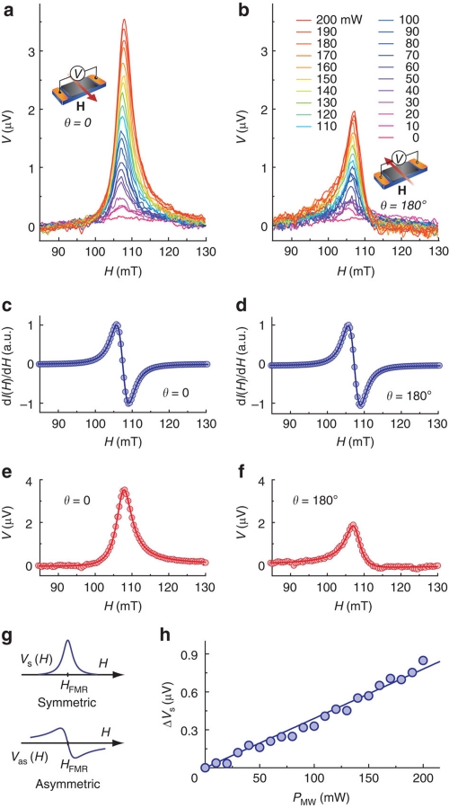
 with the parameters Vs=3.50 μV and Vas=−0.41 μV. (f) H dependence of V measured for the Ni81Fe19/p-Si film when θ=180°. The solid curve shows the fitting result with the parameters Vs=1.76 μV and Vas=0.41 μV. (g) The spectral shape of the symmetric Vs (H) and asymmetric Vas (H) components of the electromotive force V (H). (h) Microwave power PMW dependence of ΔVs, where
  . The solid circles are the experimental data. The solid line shows the linear fit to the data.
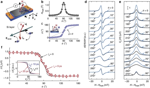
 (the black curve).
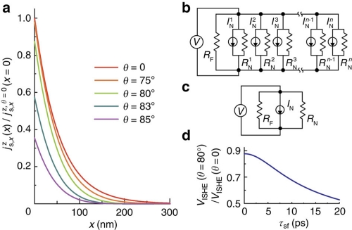
 generated by the spin pumping for τsf=9 ps. Here
  is the spin current density at the interface when the external magnetic field is applied along the film plane (θ=0). The parameters used for the calculation are shown in the text. (b) An equivalent circuit model of the Ni81Fe19/p-Si film. RF is the electrical resistance of the Ni81Fe19 layer. (c) A simplified equivalent circuit model of the Ni81Fe19/p-Si film. (d) The spin relaxation time τsf dependence of the ISHE signal VISHE at θ=80° calculated from equation (5).
References
-
- Žutić I., Fabian J. & Das Sarma S. Spintronics: fundamentals and applications. Rev. Mod. Phys. 76, 323–410 (2004).
-
- Fabian J., Matos-Abiague A., Ertler C., Stano P. & Žutić I. Semiconductor spintronics. Acta Phys. Slov. 57, 565–907 (2007).
-
- Cheng J. L., Wu M. W. & Fabian J. Theory of the spin relaxation of conduction electrons in silicon. Phys. Rev. Lett. 104, 016601 (2010). - PubMed
-
- Wolf S. A. et al.. Spintronics: a spin-based electronics vision for the future. Science 294, 1488–1495 (2001). - PubMed
-
- Johnson M. & Silsbee R. H. Interfacial charge-spin coupling: injection and detection of spin magnetization in metals. Phys. Rev. Lett. 55, 1790–1793 (1985). - PubMed
Publication types
LinkOut - more resources
Full Text Sources
Other Literature Sources
