. 2012 Feb 14:3:677.
doi: 10.1038/ncomms1682.

CMOS-based carbon nanotube pass-transistor logic integrated circuits

Affiliations
Free PMC article

CMOS-based carbon nanotube pass-transistor logic integrated circuits

Li Ding et al. Nat Commun. .
Free PMC article

Abstract

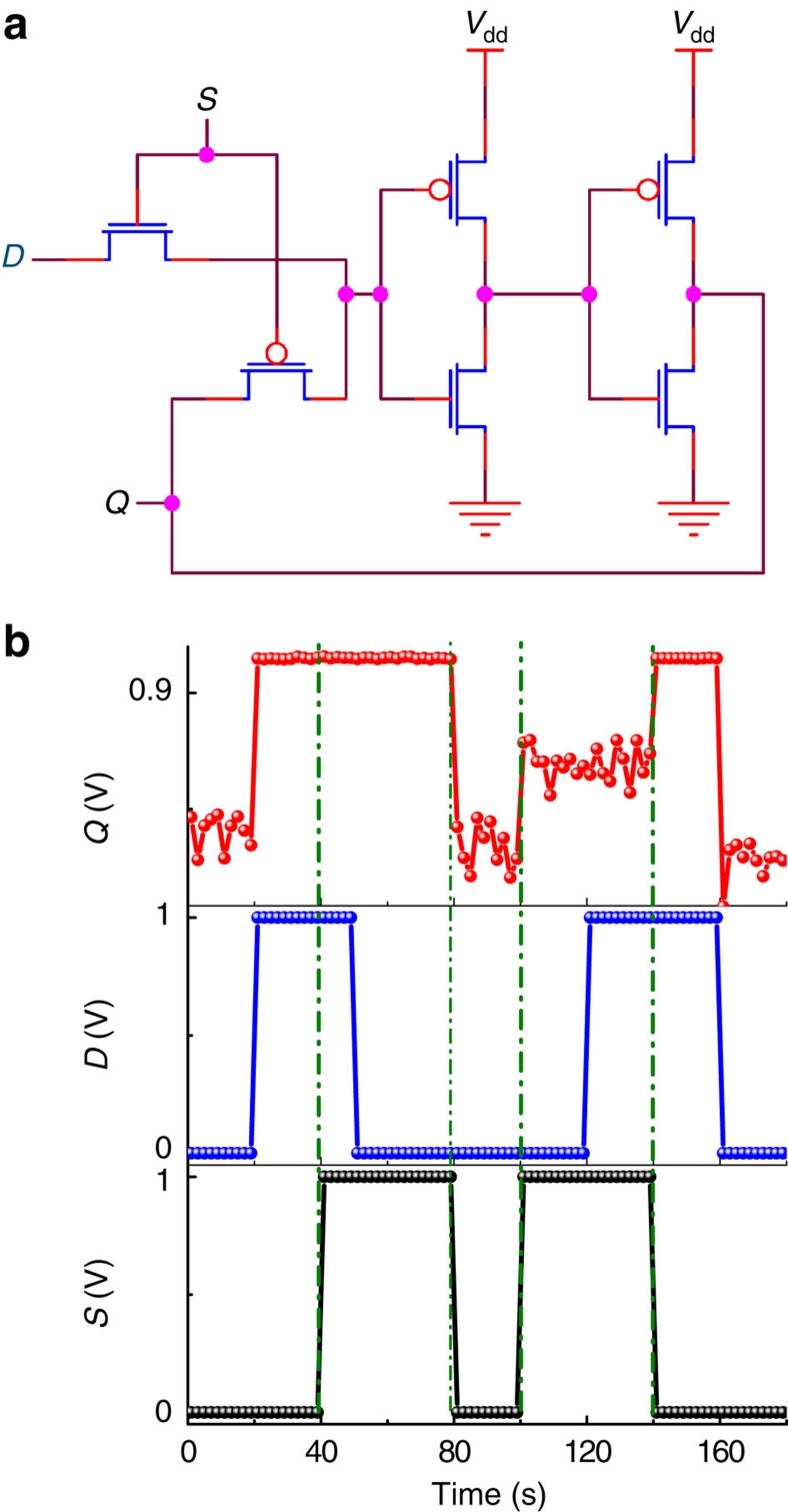
Field-effect transistors based on carbon nanotubes have been shown to be faster and less energy consuming than their silicon counterparts. However, ensuring these advantages are maintained for integrated circuits is a challenge. Here we demonstrate that a significant reduction in the use of field-effect transistors can be achieved by constructing carbon nanotube-based integrated circuits based on a pass-transistor logic configuration, rather than a complementary metal-oxide semiconductor configuration. Logic gates are constructed on individual carbon nanotubes via a doping-free approach and with a single power supply at voltages as low as 0.4 V. The pass-transistor logic configurarion provides a significant simplification of the carbon nanotube-based circuit design, a higher potential circuit speed and a significant reduction in power consumption. In particular, a full adder, which requires a total of 28 field-effect transistors to construct in the usual complementary metal-oxide semiconductor circuit, uses only three pairs of n- and p-field-effect transistors in the pass-transistor logic configuration.


Figures

Figure 1
Figure 1. Geometry and characteristics of the CNT-based FETs.
(a) A scanning electron microscopic image showing a pair of p- and n-FETs on a single CNT, scale bar is 10 μm. Shown in (b) and (c) are the transfer characteristics of the p-FET and n-FET, based on the same CNT with a diameter of approximately 1.8 nm and a channel length of approximately 1 μm. For the p-FET, the source is biased at 1.0 V and drain is at 0 V, whereas for the n-FET, the source is biased at 0 V and the drain is at 1.0 V. The olive box defines the 1 V gate voltage window used to obtain Ion, where Vth is determined using the standard peak transconductance method. The extracted Vth (violet point) and Ion (red point) are (b) 0.05 V and 10.6 μA for the p-FET, and (c) 0.03 V and 10.4 μA for the n-FET. (d) The output characteristics of the p-type (green lines) and n-type (blue lines) CNT FETs with |Vgs| varying from 0 to 1 V in steps of 0.2 V, from bottom to top.
Figure 2
Figure 2. The operating principles of CNT-based PTL circuits.
Shown in (a) and (b) are schematic diagrams (left) depicting the operating principles and experimentally measured output resistances (right) of a p-type pass-transistor (a) in the ON state, that is, biasing the gate at 0 V and (b) in the OFF state, that is, biasing the gate at 1 V, respectively. In the right panels, the blue curves denote passing a logic '1', and the olive curves denote passing a logic '0'. The dotted lines represent the case of the OFF state, whereas the solid lines represent the case of the ON state. Shown in (c) and (d) are schematic diagrams (left) depicting the operating principles and experimentally measured output resistances (right) of an n-type pass-transistor (c) in the ON state, that is, biasing the gate at 1 V and (d) in the OFF state, that is, biasing the gate at 0 V, respectively. In the right panels, the green curves denote passing a logic '0', and the blue curves denote passing a logic '1'. The solid lines represent the case of the ON state, whereas the dotted lines represent the case of the OFF state. To measure the passing of a logic '1', Vin is set to 1.0 V. Conversely, to measure the passing of a logic '0', Vin is set to 0 V.
Figure 3
Figure 3. CMOS-based pass-transistor OR and AND gates.
(a) Circuit design (top) and truth table (bottom) for an OR gate. (b) Output voltage levels for all four input states of the OR gate. (c) Circuit design (top) and truth table (bottom) for an AND gate. (d) Output voltage levels for all four input states of the AND gate.
Figure 4
Figure 4. CMOS-based pass-transistor XOR gate and a full adder.
(a) Circuit design (upper) and truth table (lower) for an XOR gate. (b) Output voltage levels for all four input states of the XOR gate. (c) Circuit design and (d) truth table for a full adder, where SUM denotes summation and Co denotes carry-out. (e) Output voltage levels for SUM and the full adder for all eight input states, and (f) output voltage levels for Co and all eight input states.
Figure 5
Figure 5. CMOS and PTL hybrid circuits.
(a) Circuit design for an XOR gate with a cascading CMOS inverter. (b) Output voltage levels for all four input states of the XOR gate without (blue spheres) and with (green spheres) a cascading CMOS inverter. (c) Circuit design for an XOR gate with a driving CMOS inverter. (d) Output voltage levels for all four input states of the XOR gate without (blue spheres) and with (green spheres) a CMOS inverter as its driving circuit.
Figure 6
Figure 6. CMOS-based two-to-one MUX and two-to-four DEMUX.
(a) Circuit design for a PTL two-to-one MUX, where S is the input control signal. (b) Experimentally measured output voltage levels for all eight input combinations of (S, A, B), and (c) the truth table of the two-to-one MUX. (d) Circuit design and (e) truth table of a PTL two-to-four DEMUX. The four outputs (D0 to D3) are selected by the combinations of (A0, A1). (f) Experimentally measured output voltage levels of the two-to-four DEMUX for all four input states of (A1, A0).
Figure 7
Figure 7. Design and characteristics of a CNT-based D-latch circuit.
(a) Circuit design with a hybrid CMOS–PTL configuration and (b) output, Q, waveforms (red), and corresponding clock (S, black) and data (D, blue) inputs.
Figure 8
Figure 8. Performance of CMOS-based PTL gates for different supply voltages.
Output voltage levels for all four input states of an OR gate at (a) VDD=1.0 and (b) 0.4 V. Output voltage levels for all four input states of an AND gate at (c) VDD=1.0 and (d) 0.4 V.

Similar articles

Cited by

References

    1. Avouris P., Chen Z. H. & Perebeinos V. Carbon-based electronics. Nat. Nanotechnol. 2, 605–615 (2007). - PubMed
    1. Rutherglen C., Jain D. & Burke P. Nanotube electronics for radiofrequency applications. Nat. Nanotechnol. 4, 811–819 (2009). - PubMed
    1. Burghard M., Klauk H. & Kern K. Carbon-based field-effect transistors for nanoelectronics. Adv. Mater. 21, 2586–2600 (2009). - PubMed
    1. Heinze S.. Carbon nanotubes as Schottky barrier transistors. Phys. Rev. Lett. 89, 106801 (2002). - PubMed
    1. Chen Z., Appenzeller J., Knoch J., Lin Y.- M. & Avouris P. The role of metal-nanotube contact in the performance of carbon nanotube field-effect transistors. Nano Lett. 5, 1497–1502 (2005). - PubMed

Publication types