. 2009;9(7):5076-8098.
doi: 10.3390/s90705076. Epub 2009 Jun 26.

Selective attention in multi-chip address-event systems

Affiliations

Selective attention in multi-chip address-event systems

Chiara Bartolozzi et al. Sensors (Basel). 2009.

Abstract

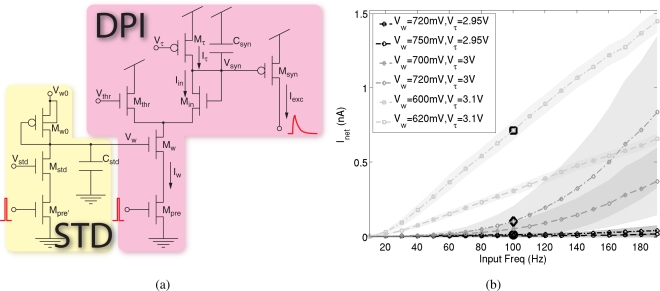
Selective attention is the strategy used by biological systems to cope with the inherent limits in their available computational resources, in order to efficiently process sensory information. The same strategy can be used in artificial systems that have to process vast amounts of sensory data with limited resources. In this paper we present a neuromorphic VLSI device, the "Selective Attention Chip" (SAC), which can be used to implement these models in multi-chip address-event systems. We also describe a real-time sensory-motor system, which integrates the SAC with a dynamic vision sensor and a robotic actuator. We present experimental results from each component in the system, and demonstrate how the complete system implements a real-time stimulus-driven selective attention model.

Keywords: Address-Event Representation (AER); analog VLSI; multi-chip system; saliency-map; selective attention; subthreshold; winner-take-all (WTA).


Figures

Figure 1.
Figure 1.
Block diagram of the SAC pixel. Each pixel receives sequences of spikes from the AER bus and competes for saliency by means of lateral connections. The winning pixel sends its address to the AER bus and self-inhibits via the inhibitory synapse.
Figure 2.
Figure 2.
Input excitatory synapse: (a) Circuit diagram of the excitatory synapse, comprising the DPI circuit and the STD circuit. (b) Mean and standard deviation (shaded areas) of the input current of the WTA cell versus the input frequency, when the DPI is stimulated with a spike train of constant frequency at 100 Hz, for different time constant and weight settings and disabled STD.
Figure 3.
Figure 3.
Current-mode hysteretic WTA circuit with diode-source degeneration “DS”, local excitation “EXC”, local inhibition “INH” and positive feedback “HYST”.
Figure 4.
Figure 4.
Hysteresis measured by observing the output activity of the I&F neuron: (a) Instantaneous input frequency of the spike train sent to pixel 1, and to pixel 2. (b) Center of mass of the chip’s activity versus the input frequency of pixel 2 for different amplitudes of the hysteretic current.
Figure 5.
Figure 5.
Lateral excitation. Spatial impulse response of the WTA resistive grid (see ”EXC” in Figure 3). The difference between the response for Vexc > 0 and the response for Vexc = Gnd is plotted. (a) Example of the spatial response for Vexc = 200 mV, (b) Cross section with mean and standard deviation of the data recorded from the pixels belonging to the same row and column as the central pixel, for different values of the bias Vexc.
Figure 6.
Figure 6.
Functional role of lateral excitation. (a) Center of mass of the activity of the array, when stimulating a single pixel with a constant frequency and a blob, for different values of the bias Vexc. The activity of all of the pixels belonging to the blob is added together, and represented as a single pixel. (b) Center of mass of the chip activity, when two blobs are stimulated. (c) Baseline activity without hysteresis, when either single pixels or blobs are stimulated.
Figure 7.
Figure 7.
I&F circuit diagram. It comprises a membrane capacitor, a constant leak “LK”, a spike generating circuit “SPK” with a positive feedback “Na” mimicking the fast activation of sodium channels and a reset and hyperpolarizing circuit that mimics the activation of late potassium channels “K”. The “ADAP” circuit implements spike frequency adaptation by calcium accumulation.
Figure 8.
Figure 8.
Inhibition of return: typical traces of the internal variables Vnet (top trace), Vmem (bottom trace), and Vior (black middle trace), recorded from one test pixel, for three combinations of inhibition weight (Vwinh) and time constant (Vτinh). (a) Vwinh = 2.42 V, Vτinh = 10 mV, (b) Vwinh = 2.58 V, Vτinh = 30 mV,(c) Vwinh = 2.44 V, Vτinh = 80 mV.
Figure 9.
Figure 9.
SaliencyToolbox: (a) Input image used for the following experiments (part of the image database of the SaliencyToolbox). (b) Saliency map relative to the input image, obtained from the SaliencyToolbox, with the default parameters. (c–d) FOA scan path generated by the SaliencyToolbox: The yellow circles are centered around each fixation point belonging to the FOA scan path, the red lines connect consecutive fixations. The radius of the yellow circles shows the size of the inhibition area. (c) Small inhibition area (d) Large inhibition area. (e–h) FOA scan path generated by the SAC superimposed on the saliency map for different settings of the IOR. (e–g): black dots show the fixation points, the grey lines connect consecutive fixations; (f–h) histogram of the visited points in the saliency map. (e–f) Slow IOR time constant. (g–h) Fast IOR time constant.
Figure 10.
Figure 10.
Visual selective attention AER multi-chip system comprising the DVS and the SAC.
Figure 11.
Figure 11.
Selective attention multi-chip system: (a) Experimental setup: In front of the DVS, over a white background, a LED (red circle) is flickering and a nut (red dashed arrow) is let oscillating. (b–c) The raster plots show the activity of the SAC (black dots) superimposed to the activity of the DVS (grey dots): Each dot corresponds to a spike emitted by the pixel with address on y-axis at the time indicated on the x-axis. The spikes with addresses ranging from about 1200 to 1500 correspond to the LED evoked activity, the spikes with addresses belonging to the range from ca. 2800 to ca. 3500 correspond to the nut swing. On the left the activity is plotted for 50 s. The right column corresponds to the time zoom over three seconds right after the LED turning on. (b) Baseline experiment: competition, lateral excitation, hysteresis, and IOR, are turned off. (c) WTA competition, IOR (Vτinh = 80 mV, Vthrinh = 200 mV, Vwinh = 2.4 V) and STD (Vwstd = 280 mV). (d) WTA competition, IOR turned off, STD (Vwstd = 280 mV).
Figure 12.
Figure 12.
Overt attention with moving natural stimuli: two sequences of movement (yellow arrow), target selection (red circle), saccade movement and landing (red arrow), when a person is walking to the left (upper sequence) and to the right (lower sequence).

References

    1. Lichtsteiner P., Delbrück T., Posch C. A 100 db dynamic range high-speed dual-line optical transient sensor with asynchronous readout. Proceedings of IEEE International Symposium on Circuits and Systems; 2006. IEEE,
    1. Laughlin S., Sejnowski T. Communication in neuronal networks. Science. 2003;301:1870–1874. - PMC - PubMed
    1. Turrigiano G. Homeostatic plasticity in neural networks: the more things change, the more they stay the same. Trends Neurosci. 1999;22:221–227. - PubMed
    1. Mead C. Neuromorphic electronic systems. Proceedings of the IEEE. 1990;78:1629–1936.
    1. Itti L., Niebur E., Koch C. A model of saliency-based visual attention for rapid scene analysis. IEEE Trans. Pattern Anal. Machine Intell. 1998;20:1254–1259.

LinkOut - more resources