. 2012 Feb 21:3:692.
doi: 10.1038/ncomms1691.

Broadband omnidirectional antireflection coating based on subwavelength surface Mie resonators

Affiliations

Broadband omnidirectional antireflection coating based on subwavelength surface Mie resonators

P Spinelli et al. Nat Commun. .

Abstract

Reflection is a natural phenomenon that occurs when light passes the interface between materials with different refractive index. In many applications, such as solar cells or photodetectors, reflection is an unwanted loss process. Many ways to reduce reflection from a substrate have been investigated so far, including dielectric interference coatings, surface texturing, adiabatic index matching and scattering from plasmonic nanoparticles. Here we present an entirely new concept that suppresses the reflection of light from a silicon surface over a broad spectral range. A two-dimensional periodic array of subwavelength silicon nanocylinders designed to possess strongly substrate-coupled Mie resonances yields almost zero total reflectance over the entire spectral range from the ultraviolet to the near-infrared. This new antireflection concept relies on the strong forward scattering that occurs when a scattering structure is placed in close proximity to a high-index substrate with a high optical density of states.


Figures
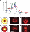
Figure 1
Figure 1. Mie scattering on a Si wafer.
(a) Scattering cross-sections, normalized to the geometrical cross-section, for a Si sphere in air (blue), a Si sphere on a Si substrate (green) and a Si cylinder on a Si substrate (red). The spheres have diameter d=150 nm, the cylinder has an in-plane diameter of 150 nm and height of 100 nm. Mie resonances of first (n=1) and second (n=2) order are indicated in the figure. (bg) Electric field intensity (colour scale) in a cross-section of the particle for a sphere in air (b,e), a sphere on substrate (c,f) and a cylinder on substrate (d,g), for Mie modes of first (bd) and second (eg) order. The wavelengths considered for these calculations are indicated in each panel. The field distribution for the cylinder at resonance overlaps with the substrate, thus introducing a loss channel for the light confined in the particle that broadens the resonances. Plots for a sphere in air are calculated with Mie theory; plots for particles on a substrate are simulated. The scale bar in e represents 50 nm, and refers to b and e. The scale bar in f represents 150 nm and refers to c,d,f and g.
Figure 2
Figure 2. Ultra-low reflectivities.
(a) Simulated reflection spectra from a regular square array of Si NPs spaced by 500 nm, for cylinder diameters of 150 (blue), 200 (red) and 250 nm (green) with a height of 150 nm. Reflectance from a flat Si surface is also shown for comparison (black). The Si NP arrays reduce the reflectivity over the entire spectrum. The broad dip in reflectivity that redshifts for increasing particle diameter is due to enhanced forward scattering from the Mie resonances in the particle. (b) Simulated reflection spectra for a bare flat Si substrate (black), a flat Si substrate coated with a standard Si3N4 antireflection coating (blue, thickness t=80 nm), a Si surface with bare Si nanostructures on top (red) and a Si surface with Si nanostructures on top coated with an optimized Si3N4 layer (green, t=50 nm). For each configuration the average reflectivity, R, weighted with the AM1.5 solar spectrum in the 300–1,100 nm spectral range, is indicated. (c) Measured total reflectivity of a bare Si wafer (black), an uncoated Si NP array (red) and four Si NP array coated with Si3N4 layers of different thicknesses, t (colours). The Si NPs have a diameter of 125 nm, height of 150 nm and are spaced by 450 nm. For each configuration the average reflectivity, R, weighted with the AM1.5 solar spectrum in the 450–900 nm spectral range, is indicated. Reflectance is reduced over the entire spectral range, due to coupling of the Mie resonant scattering to the Si substrate. (d) The same reflectivity data plotted in logarithmic scale. Individual curves are described in legend to Figure 3c. The effect of the Mie resonance is visible in the broad dip in reflectivity observed in the 700–800 nm range.
Figure 3
Figure 3. Black silicon.
(a) Photograph of a bare flat 4-inch Si wafer (left) and a 4-inch Si wafer fully imprinted with an optimized (250 nm diameter, 150 nm height, 450 nm pitch) Si NP array and overcoated with a 60-nm-thick Si3N4 layer (right). Scale bar represents 1 inch. (b) Scanning electron microscopy image taken under an angle of 40° of a bare Si NP array (scale bar represents 500 nm) and (c) a Si NP array coated with a 60-nm-thick Si3N4 layer (scale bar represents 1 μm).
Figure 4
Figure 4. Angle resolved reflectivity.
Specular reflectivity measured as a function of AOI, for wavelengths of 514 nm (a,d), 632 nm (b,e) and 405 nm (c,f). Panels in the top row show results for s- (solid symbols) and p-polarized (open symbols) incident beam, whereas the bottom row show an average of s- and p-polarizations, plotted on a logarithmic scale. In each graph, reflectivities from a bare Si wafer (black lines), a 60-nm standard Si3N4 coating (red) and a coated NP array (blue) are shown. The excellent AR properties of Si NP arrays are maintained over the entire range of AOI from −60° to +60°.

References

    1. Nature?s guiding light. Nat. Photon 2, 639 (2008).
    1. Gevaux D. Reflection! What reflection? Nat. Photon 1, 186 (2007).
    1. Macleod H. A. Thin-Film Optical Filters (Elsevier, 1969).
    1. Lamers M.W.P.E. et al.. 17.9% Metal-wrap-through mc-Si cells resulting in module efciency of 17.0%. Prog. Photovolt: Res. Appl. 20, 62–73 (2012).
    1. Southwell W. H. Pyramid-array surface-relief structures producing antireflection index matching on optical surfaces. J. Opt. Soc. Am. 8, 549–553 (1991).

Publication types