. 2012 Mar 14;7(1):187.
doi: 10.1186/1556-276X-7-187.

Effect of non-lattice oxygen on ZrO2-based resistive switching memory

Affiliations

Effect of non-lattice oxygen on ZrO2-based resistive switching memory

Chun-Chieh Lin et al. Nanoscale Res Lett. .

Abstract

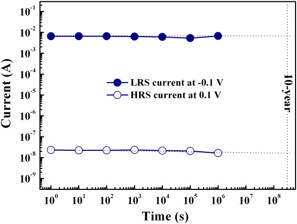
ZrO2-based resistive switching memory has attracted much attention according to its possible application in the next-generation nonvolatile memory. The Al/ZrO2/Pt resistive switching memory with bipolar resistive switching behavior is revealed in this work. The thickness of the ZrO2 film is only 20 nm. The device yield improved by the non-lattice oxygen existing in the ZrO2 film deposited at room temperature is firstly proposed. The stable resistive switching behavior and the long retention time with a large current ratio are also observed. Furthermore, it is demonstrated that the resistive switching mechanism agrees with the formation and rupture of a conductive filament in the ZrO2 film. In addition, the Al/ZrO2/Pt resistive switching memory is also possible for application in flexible electronic equipment because it can be fully fabricated at room temperature.


Figures

Figure 1
Figure 1
Structure of the Al/ZrO2/Pt device. Throughout the electrical measurements, bias voltages were applied on the Al TE; meanwhile, the Pt BE was grounded.
Figure 2
Figure 2
Typical resistive switching I-V curves of the Al/ZrO2/Pt device. Under the bipolar resistive switching mode (curves 1 and 2) and the unipolar resistive switching mode (curves 1 and 3).
Figure 3
Figure 3
Yields of the Al/ZrO2/Pt samples deposited at various temperatures. Where the ZrO2 films were deposited at RT, 150°C, 200°C, 250°C, and 300°C. The samples fabricated at RT show the highest yield.
Figure 4
Figure 4
XPS spectra of the ZrO2 films deposited at various temperatures. (a) Zr 3d and (b) O 1s XPS spectra of the ZrO2 films deposited at RT, 150°C, 200°C, 250°C, and 300°C. The ZrO2 film deposited at RT possesses the highest content of the non-lattice oxygen.
Figure 5
Figure 5
Resistive switching cycles of the samples fabricated at RT. Under the (a) bipolar and (b) unipolar modes. The resistive switching can be stably repeated for over 100 times under both resistive switching modes.
Figure 6
Figure 6
Cumulative probabilities of the set and reset voltages and the LRS and HRS currents. Cumulative probabilities of the set and reset voltages of the sample fabricated at RT under the (a) bipolar and (b) unipolar modes. The set and reset voltages under the bipolar mode are distinguishable. (c) Cumulative probabilities of the HRS currents measured at 0.1 V and the LRS currents measured at -0.1 V under the bipolar mode. Two memory states are distinguishable.
Figure 7
Figure 7
Retention time of the sample fabricated at RT. LRS and HRS currents measured at ± 0.1 V firmly hold on about 6 mA and 2 × 10⁻⁸ A, respectively, for over 106 s without applying any power supply, so the good nonvolatility of the sample is demonstrated.
Figure 8
Figure 8
Device-to-device uniformities of ten samples fabricated at RT under the bipolar resistive switching mode. Including the set and reset voltages and the LRS and HRS currents measured at ± 0.1 V.
Figure 9
Figure 9
Possible resistive switching mechanism of the Al/ZrO2/Pt device. The set and reset are due to the formation and rupture of the CF in the ZrO2 film.

References

    1. Baek IG, Lee MS, Seo S, Lee MJ, Seo DH, Suh DS, Park JC, Park SO, Kim HS, Yoo IK, Chung UI, Moon JT. Highly scalable non-volatile resistive memory using simple binary oxide driven by asymmetric unipolar voltage pulses. IEDM Tech Dig. 2004. p. 587.
    1. Chen A, Haddad S, Wu YC, Fang TN, Lan Z, Avanzino S, Pangrle S, Buynoski M, Rathor M, Cai W, Tripsas N, Bill C, VanBuskirk M, Taguchi M. Non-volatile resistive switching for advanced memory applications. IEDM Tech Dig. 2005. p. 746.
    1. Lee HY, Chen PS, Wu TY, Chen YS, Wang CC, Tzeng PJ, Lin CH, Chen F, Lien CH, Tsai MJ. Low power and high speed bipolar switching with a thin reactive Ti buffer layer in robust HfO2 based RRAM. IEDM Tech Dig. 2008. p. 1.
    1. Zhang T, Zhang X, Ding L, Zhang W. Study on resistance switching properties of Na0.5Bi0.5TiO3 thin films using impedance spectroscopy. Nanoscale Res Lett. 2009;4:1309–1314. doi: 10.1007/s11671-009-9397-4. - DOI - PMC - PubMed
    1. Li Y, Long S, Zhang M, Liu Q, Shao L, Zhang S, Wang Y, Zuo Q, Liu S, Liu M. Resistive switching properties of Au/ZrO2/Ag structure for low-voltage nonvolatile memory applications. IEEE Electron Device Lett. 2010;31:117–119.

LinkOut - more resources