. 2012:2:349.
doi: 10.1038/srep00349. Epub 2012 Apr 2.

III-V/Si hybrid photonic devices by direct fusion bonding

III-V/Si hybrid photonic devices by direct fusion bonding

Katsuaki Tanabe et al. Sci Rep. 2012.

Abstract

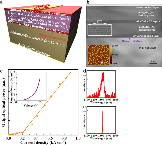
Monolithic integration of III-V compound semiconductors on silicon is highly sought after for high-speed, low-power-consumption silicon photonics and low-cost, light-weight photovoltaics. Here we present a GaAs/Si direct fusion bonding technique to provide highly conductive and transparent heterojunctions by heterointerfacial band engineering in relation to doping concentrations. Metal- and oxide-free GaAs/Si ohmic heterojunctions have been formed at 300°C; sufficiently low to inhibit active material degradation. We have demonstrated 1.3 μm InAs/GaAs quantum dot lasers on Si substrates with the lowest threshold current density of any laser on Si to date, and AlGaAs/Si dual-junction solar cells, by p-GaAs/p-Si and p-GaAs/n-Si bonding, respectively. Our direct semiconductor bonding technique opens up a new pathway for realizing ultrahigh efficiency multijunction solar cells with ideal bandgap combinations that are free from lattice-match restrictions required in conventional heteroepitaxy, as well as enabling the creation of novel high performance and practical optoelectronic devices by III-V/Si hybrid integration.


Figures

Figure 1
Figure 1. GaAs/Si direct wafer bonding.
(a) Configuration schematic of the I–V measurement for the direct-bonded GaAs/Si heterointerfacial electrical characteristics. A positive bias voltage was applied from the GaAs side. (b, c) I–V characteristics of the direct-bonded GaAs/Si heterointerfaces with varying doping concentrations and bonding temperature. (d, e) Calculated profiles of the conduction and valence band edges across the (d) p-GaAs/p-Si and (e) p-GaAs/n-Si heterointerfaces with varying doping concentrations. The inset in e shows a closeup around the origin. (f) Cross-sectional transmission electron microscope image of a direct-bonded p+-GaAs/p+-Si heterointerface. (g–i) Selected-area diffraction patterns at the same heterointerface as of f for regions around 70 nm in radius centred (g) 80 nm above the interface, (h) at the interface, and (i) 80 nm below the interface, identified as single-crystal GaAs, a mixture of single-crystal GaAs and Si, and single-crystal Si, respectively.
Figure 2
Figure 2. InAs/GaAs quantum dot laser on Si substrate.
(a) Cross-sectional schematic diagram of the fabricated InAs/GaAs quantum dot laser on a Si substrate. The thickness and doping concentration of each layer are indicated. The abbreviations QD and ND stand for quantum dot and non-doped, respectively. (b) Cross-sectional transmission electron microscope image of the laser. The upper inset shows a detailed image of the InAs/GaAs quantum dot layers. The lower inset shows an atomic force microscope image of the as-grown InAs/GaAs quantum dots. (c) Light-current characteristics of the laser for pulsed electrical pumping at room temperature. The I–V characteristics of the laser are shown in the inset. (d, e) Electroluminescence spectra of the laser at current densities of 140 (below the lasing threshold) and 380 (above the lasing threshold) A cm−2, respectively.
Figure 3
Figure 3. AlGaAs/Si dual-junction solar cell.
(a) Cross-sectional schematic diagram of the fabricated AlGaAs/Si dual-junction solar cell. The thickness and doping concentration of each layer are indicated. The abbreviation BSF stands for back surface field. (b) Cross-sectional scanning electron microscope image of the solar cell. Inset shows the light I–V and power-voltage characteristics of the solar cell under a 600 nm-peaked halogen white light source of a one-sun intensity (100 mW cm−2).

References

    1. Seassal C. et al. InP microdisk lasers on silicon wafer: CW room temperature operation at 1.6 μm. Electron. Lett. 37, 222–223 (2001).
    1. Monat C. et al. InP-based two-dimensional photonic crystal on silicon: In-plane Bloch mode laser. Appl. Phys. Lett. 81, 5102–5104 (2002).
    1. Palit S. et al. Low-threshold thin-film III-V lasers bonded to silicon with front and back side defined features. Opt. Lett. 34, 2802–2804 (2009). - PubMed
    1. Tanabe K., Nomura M., Guimard D., Iwamoto S. & Arakawa Y. Room temperature continuous wave operation of InAs/GaAs quantum dot photonic crystal nanocavity laser on silicon substrate. Opt. Express 17, 7036–7042 (2009). - PubMed
    1. Tanabe K., Guimard D., Bordel D., Iwamoto S. & Arakawa Y. Electrically pumped 1.3 μm room-temperature InAs/GaAs quantum dot lasers on Si substrates by metal-mediated wafer bonding and layer transfer. Opt. Express 18, 10604–10608 (2010). - PubMed