

Multifunctional graphene woven fabrics
- PMID: 22563524
- PMCID: PMC3343323
- DOI: 10.1038/srep00395
Multifunctional graphene woven fabrics
Abstract
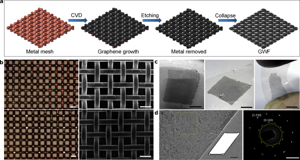
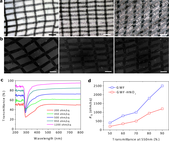
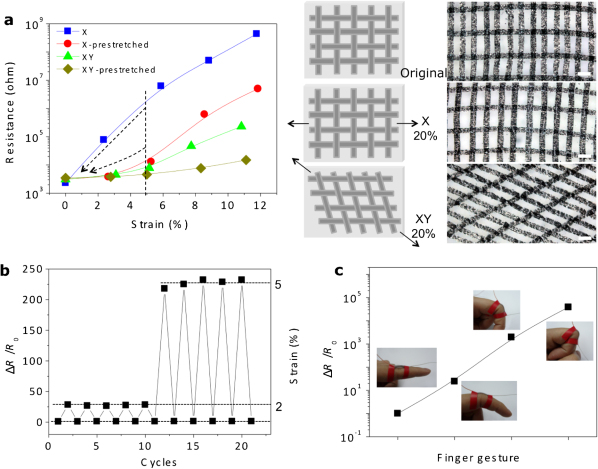
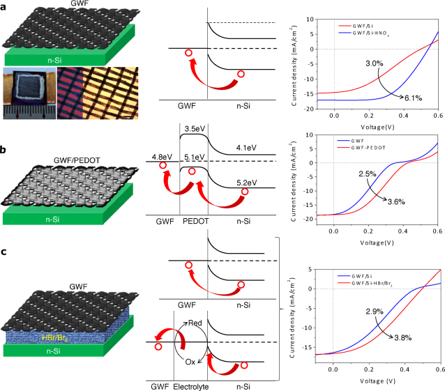
Tailoring and assembling graphene into functional macrostructures with well-defined configuration are key for many promising applications. We report on a graphene-based woven fabric (GWF) prepared by interlacing two sets of graphene micron-ribbons where the ribbons pass each other essentially at right angles. By using a woven copper mesh as the template, the GWF grown from chemical vapour deposition retains the network configuration of the copper mesh. Embedded into polymer matrices, it has significant flexibility and strength gains compared with CVD grown graphene films. The GWFs display both good dimensional stability in both the warp and the weft directions and the combination of film transparency and conductivity could be optimized by tuning the ribbon packing density. The GWF creates a platform to integrate a large variety of applications, e.g., composites, strain sensors and solar cells, by taking advantages of the special structure and properties of graphene.
Figures
Similar articles
-
Planar Porous Graphene Woven Fabric/Epoxy Composites with Exceptional Electrical, Mechanical Properties, and Fracture Toughness.ACS Appl Mater Interfaces. 2015 Sep 30;7(38):21455-64. doi: 10.1021/acsami.5b06476. Epub 2015 Sep 15. ACS Appl Mater Interfaces. 2015. PMID: 26331902
-
Tactile Sensing System Based on Arrays of Graphene Woven Microfabrics: Electromechanical Behavior and Electronic Skin Application.ACS Nano. 2015 Nov 24;9(11):10867-75. doi: 10.1021/acsnano.5b03851. Epub 2015 Oct 16. ACS Nano. 2015. PMID: 26468735
-
Spider-Web-Inspired Stretchable Graphene Woven Fabric for Highly Sensitive, Transparent, Wearable Strain Sensors.ACS Appl Mater Interfaces. 2019 Jan 16;11(2):2282-2294. doi: 10.1021/acsami.8b18312. Epub 2019 Jan 7. ACS Appl Mater Interfaces. 2019. PMID: 30582684
-
Transparent Conductive Electrodes Based on Graphene-Related Materials.Micromachines (Basel). 2018 Dec 26;10(1):13. doi: 10.3390/mi10010013. Micromachines (Basel). 2018. PMID: 30587828 Free PMC article. Review.
-
A Comprehensive Review on Advanced Sustainable Woven Natural Fibre Polymer Composites.Polymers (Basel). 2021 Feb 2;13(3):471. doi: 10.3390/polym13030471. Polymers (Basel). 2021. PMID: 33540731 Free PMC article. Review.
Cited by
-
Lab-on-a-Contact Lens: Recent Advances and Future Opportunities in Diagnostics and Therapeutics.Adv Mater. 2022 Jun;34(24):e2108389. doi: 10.1002/adma.202108389. Epub 2022 Apr 11. Adv Mater. 2022. PMID: 35130584 Free PMC article. Review.
-
Multifunctional non-woven fabrics of interfused graphene fibres.Nat Commun. 2016 Nov 30;7:13684. doi: 10.1038/ncomms13684. Nat Commun. 2016. PMID: 27901022 Free PMC article.
-
Freestanding Graphene Fabric Film for Flexible Infrared Camouflage.Adv Sci (Weinh). 2022 Feb;9(5):e2105004. doi: 10.1002/advs.202105004. Epub 2021 Dec 16. Adv Sci (Weinh). 2022. PMID: 34914865 Free PMC article.
-
Mechanical sensors based on two-dimensional materials: Sensing mechanisms, structural designs and wearable applications.iScience. 2022 Jan 1;25(1):103728. doi: 10.1016/j.isci.2021.103728. eCollection 2022 Jan 21. iScience. 2022. PMID: 35072014 Free PMC article. Review.
-
Stretchable and highly sensitive graphene-on-polymer strain sensors.Sci Rep. 2012;2:870. doi: 10.1038/srep00870. Epub 2012 Nov 16. Sci Rep. 2012. PMID: 23162694 Free PMC article.
References
-
- Li Y., Qian F., Xiang J. & Lieber C. M. Nanowire electronic and optoelectronic devices. Mater. Today 9, 18–27 (2006).
-
- Avouris P. & Chen J. Nanotube electronics and optoelectronics. Mater. Today 9, 46–54 (2006).
-
- Rueckes T., Kim K., Joselevich E., Tseng G. Y., Cheung C. L. & Lieber C. M. Carbon nanotube-based nonvolatile random access memory for molecular computing. Science 289, 94–97 (2000). - PubMed
-
- Chen Z. H., Appenzeller J., Lin Y. M., Sippel-Oakley J., Rinzler A. G., Tang J. Y., Wind S. J., Solomon P. M. & Avouris P. An integrated logic circuit assembled on a single carbon nanotube. Science 311, 1735–1735 (2006). - PubMed
-
- Yao J., Liu Z. W., Liu Y. M., Wang Y., Sun C., Bartal G., Stacy A. M. & Zhang X. Optical negative refraction in bulk metamaterials of nanowires. Science 321, 930–930 (2008). - PubMed
LinkOut - more resources
Full Text Sources
Other Literature Sources
