. 2011 Dec 1;36(12):1052-1063.
doi: 10.1557/mrs.2011.269.

Semiconductor nanowires: A platform for nanoscience and nanotechnology

Affiliations

Semiconductor nanowires: A platform for nanoscience and nanotechnology

Charles M Lieber. MRS Bull. .

Abstract

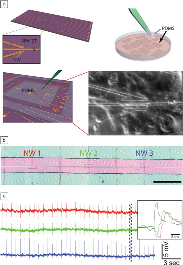
Advances in nanoscience and nanotechnology critically depend on the development of nanostructures whose properties are controlled during synthesis. We focus on this critical concept using semiconductor nanowires, which provide the capability through design and rational synthesis to realize unprecedented structural and functional complexity in building blocks as a platform material. First, a brief review of the synthesis of complex modulated nanowires in which rational design and synthesis can be used to precisely control composition, structure, and, most recently, structural topology is discussed. Second, the unique functional characteristics emerging from our exquisite control of nanowire materials are illustrated using several selected examples from nanoelectronics and nano-enabled energy. Finally, the remarkable power of nanowire building blocks is further highlighted through their capability to create unprecedented, active electronic interfaces with biological systems. Recent work pushing the limits of both multiplexed extracellular recording at the single-cell level and the first examples of intracellular recording is described, as well as the prospects for truly blurring the distinction between nonliving nanoelectronic and living biological systems.


Figures

Figure 1
Figure 1
Basic semiconductor nanowire classes realized by nanocluster-catalyzed vapor-liquid-solid growth. (center) Parent nanowire structure consists of uniform composition and doping (green) and diameter; the nanocluster catalyst (golden) is highlighted at the left tip of the structure. (clockwise from lower left) Axial nanowire with composition and/or doping (indicated by different colors) modulated during elongation of the structure; core/shell or coaxial nanowire with composition and/or doping (indicated by different colors) modulated by sequential two-dimensional shell growth following axial elongation; branched or tree-like nanowire with unique composition and/or doping branches are elaborated by sequential nanocluster-catalyzed growth; and a kinked-nanowire with structurally coherent “kinks” introduced in a controlled manner during axial elongation.
Figure 2
Figure 2
(a) Schematics of two distinct motifs for nanowire photovoltaics where the single p -type/intrinsic/ n-type (p-i-n) diodes are synthetically integrated in (top) axial and (bottom) core/shell structures. (b) Scanning electron microscopy (SEM) images of p-i-n silicon nanowires. (top) As-grown nanowire with nanocluster catalyst on right tip of nanowire. (bottom) Dopant-selective etched nanowire highlighting the distinct p-, i-, and n-type regions with lengths consistent with growth times. (c) SEM images of a p-i-n coaxial silicon nanowire at different magnifications. Images were recorded with the electron beam (left) perpendicular to the nanowire axis and (right) nearly end on. Adapted from References –.
Figure 3
Figure 3
(a) Dark current versus voltage (I–V) curves of a p-i-n core/shell device with contacts on core–core, shell–shell, and different core–shell combinations; Vbias is the applied voltage. Inset, optical microscope image of the device; scale bar, 5 μm. (b) Dark and light I–V curves recorded for the coaxial nanowire device, where the light curve was recorded under 1-sun illumination. (c) Cross-sectional schematics of four distinct core/shell diode geometries investigated as standalone single nanowire solar cells. The core in all structures is p-type. (d) Normalized (photocurrent/short-circuit photocurrent) light I–V characteristics of single nanowire solar cells corresponding to the four distinct diode geometries shown in (c). Adapted from Reference .
Figure 4
Figure 4
External quantum efficiency (EQE) as a function of wavelength for a p-i-n nanowire (black curve) and simulated EQE spectrum (dashed red curve) produced with no adjustable parameter other than the size of the nanowire (height of 240 nm). Dashed green curve shows the simulated spectrum for the top 240 nm of planar Si. (inset) Plot of electric field intensity for a plane wave (λ = 445 nm) interacting with a Si nanowire (top) and thin film (bottom). White line defines outline of nanowire and top surface of the thin film. To the right are plots of total short-circuit current density (JSC) as a function of position inside the nanowire and thin film.
Figure 5
Figure 5
(a) (top left) Nanowire field-effect transistor (NWFET) chip, where nanowire devices are located at the central region of the chip. The visible linear features (gold) correspond to nanowire contacts and interconnect metal. Zoom-in showing a source, S, and two drain electrodes, D, connected to a vertically oriented nanowire (green arrow) defining two NWFETs. (top right) Cells cultured on thin rectangular pieces of poly(dimethylsiloxane) (PDMS), where the black arrow highlights one piece in the culture medium, and the gray arrow indicates one piece being removed with tweezers. (bottom) PDMS piece with cultured cells oriented over the device region of a NWFET chip. The green needle-like structure indicates the probe used to manipulate the PDMS/cell substrate to specific nanowire device locations. (lower right) Optical micrograph of the assembly in cell medium for the area corresponding to the zoom-in in the image on the top left. (b) Optical micrograph showing three NWFET devices (NW1, NW2, NW3) in a linear array, where pink indicates the area with exposed devices; scale bar, 150 μm. (c) Representative conductance versus time signals recorded from spontaneously beating cardiomyocytes by NW1, NW2, and NW3. Inset, high-resolution comparison of the temporally correlated peaks highlighted by the dashed box. Adapted from Reference .
Figure 6
Figure 6
(a) Overview of a nanowire field-effect transistor (NWFET) array fabricated on a transparent substrate with an acute brain-slice oriented with the pyramidal cell layer over the devices. (b) Laminar organization and input circuitry of the piriform cortex in the region of the brain slice oriented over the NWFET array. (c) Optical image of an acute slice over a 4 × 4 NWFET array. Signals were recorded simultaneously from the eight devices indicated on the image. Crosses along the lateral olfactory tract fiber region (dark band at bottom of image) of the slice mark the stimulation spots a–h. Scale bar is 100 μm. (d) Maps of the relative signal intensity or activity for devices 1–8 obtained following near threshold stimulation at sites a–h. Adapted from Reference .
Figure 7
Figure 7
(a) Scanning electron microscopy (SEM) image of a multiply kinked two-dimensional silicon nanowire with equal ca. 0.8 μm arm segment lengths. The nanocluster catalyst is evident at the right end as the bright/high-contrast dot. (b) Atomic force microscopy (top) and scanning gate microscopy (SGM) (bottom panels) images of one dopant-modulated double-kinked silicon nanowire structure. The SGM images were recorded with a tip-voltage, Vtip, of +10 V (left) and –10 V (right). The dark and bright regions correspond to reduced and enhanced conductance, respectively. The black dashed lines mark the nanowire position, and the arrows point to the position of the lightly doped active region of the device. (c) Schematics of 60° cis (top) and trans (bottom) configurations for double-kinked nanowires. The blue and pink regions designate the source/drain (S/D) and nanoscale field-effect transistor (FET) channel, respectively. (right) SEM image of a double-kinked nanowire with a cis kink configuration. L is the length of segment between two adjacent kinks. Adapted from References and .
Figure 8
Figure 8
(a) Schematics of a nanowire probe as it (left) approaches and (middle) contacts the outer membrane surface and (right) enters a cell. Dark purple, light purple, pink, and blue colors denote the phospholipid bilayers, heavily doped nanowire segments, active sensor segment, and cytosol, respectively. (b) Differential interference contrast microscopy images (upper panels) and electrical recording (lower panel) of an HL-1 cell and 60° kinked nanowire probe as the cell approaches (left), contacts and internalizes (middle), and is retracted from (right) the nanoprobe. A pulled-glass micropipette (inner tip diameter ~5 μm) was used to manipulate and voltage clamp the HL-1 cell. The dashed green line corresponds to the micropipette potential. Scale bars, 5 μm. Adapted from Reference .
Figure 9
Figure 9
(a) Schematics of cellular recording highlighting the extracellular (left) and intracellular (right) nanowire/cell interfaces. The cell membrane and nanowire lipid coatings are marked with purple lines. (b) Electrical recording from beating cardiomyocytes: (top) extracellular recording and (bottom) steady-state intracellular recording. The red-dashed box indicates the region selected for (c). (c) Single high-resolution action potential peak recorded with the kinked-nanowire bioprobe. Blue and orange stars designate features that are associated with inward sodium and outward potassium currents, respectively. The letters a–e denote five characteristic phases of a cardiac intracellular potential, as defined in text. The red-dashed line is the baseline corresponding to intracellular resting state. (d) Schematic of a kinked-nanowire electronic sensor probing the intracellular region of a cell. Adapted from Reference .
Figure 10
Figure 10
Cyborg cardiac tissue (red) in which a three-dimensional nanowire field-effect transistor network is seamlessly integrated with three-dimensional cultured cardiomyocytes. The width and thickness of the cyborg tissue are ca. 2.5 cm and 1 mm, respectively.

References

    1. Lieber CM, Morales AM, Sheehan PE, Wong EW, Yang P. In: Proceedings of the Robert A. Welch Foundation 40th Conference on Chemical Research: Chemistry on the Nanometer Scale. Robert A, editor. Welch Foundation; 1997. pp. 165–187.
    1. Morales AM, Lieber CM. Science. 1998;279:208. - PubMed
    1. Hu J, Ouyang M, Yang P, Lieber CM. Nature. 1999;399:48.
    1. Duan X, Lieber CM. J. Am. Chem. Soc. 2000;122:188.
    1. Duan X, Wang J, Lieber CM. Appl. Phys. Lett. 2000;76:1116.

LinkOut - more resources