. 2012 Jul 17;109(29):11588-92.
doi: 10.1073/pnas.1205696109. Epub 2012 Jul 2.

High-frequency self-aligned graphene transistors with transferred gate stacks

Affiliations

High-frequency self-aligned graphene transistors with transferred gate stacks

Rui Cheng et al. Proc Natl Acad Sci U S A. .

Abstract

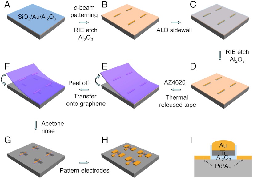
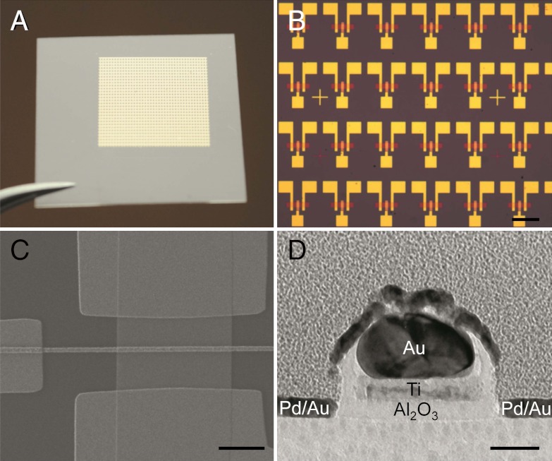
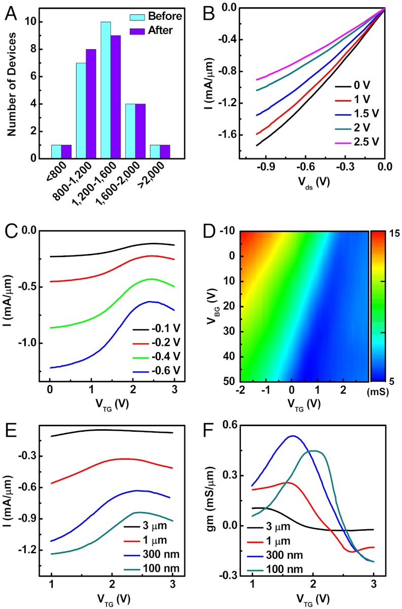
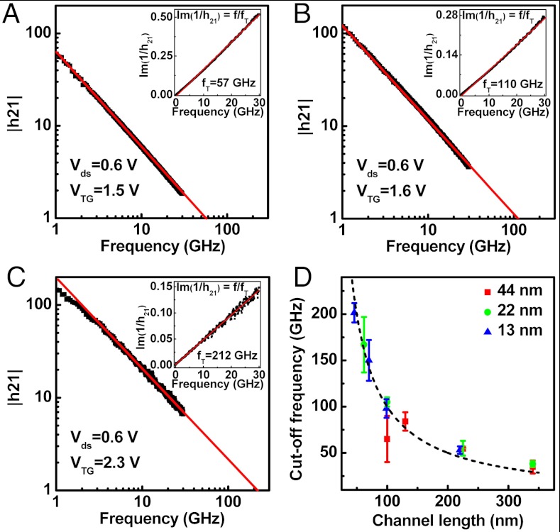
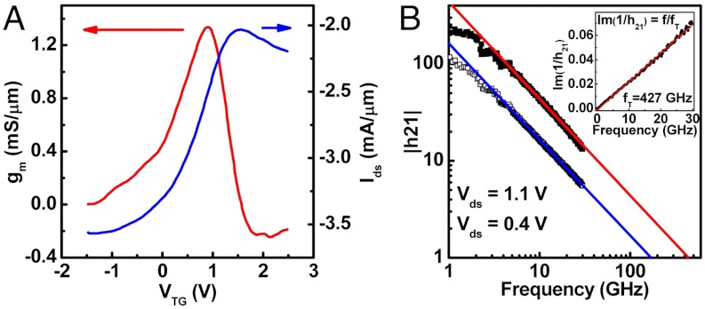
Graphene has attracted enormous attention for radio-frequency transistor applications because of its exceptional high carrier mobility, high carrier saturation velocity, and large critical current density. Herein we report a new approach for the scalable fabrication of high-performance graphene transistors with transferred gate stacks. Specifically, arrays of gate stacks are first patterned on a sacrificial substrate, and then transferred onto arbitrary substrates with graphene on top. A self-aligned process, enabled by the unique structure of the transferred gate stacks, is then used to position precisely the source and drain electrodes with minimized access resistance or parasitic capacitance. This process has therefore enabled scalable fabrication of self-aligned graphene transistors with unprecedented performance including a record-high cutoff frequency up to 427 GHz. Our study defines a unique pathway to large-scale fabrication of high-performance graphene transistors, and holds significant potential for future application of graphene-based devices in ultra-high-frequency circuits.


Conflict of interest statement

The authors declare no conflict of interest.

Figures

Fig. 1.
Fig. 1.
Schematic illustration of the fabrication of self-aligned graphene transistors with transferred gate stacks. (A) A 50-nm gold film is first deposited on a Si/SiO2 substrate by e-beam evaporation followed by a standard ALD of Al2O3 film. (B) RIE process is employed to pattern the dielectric strips after standard lithography and metallization process. (C) The gate sidewall spacer is formed by depositing a thin-layer Al2O3 film using ALD approach. (D) An anisotropic RIE process is used to etch away unwanted Al2O3 film on the top surface of the gate metal and the substrate. (E) A layer of polymer that has glass transition temperature close to the thermal tape–releasing temperature is spin-cast before applying thermal releasing tape and peeling off the gate stacking. (F) The patterned top-gate stacks are peeled from the Si wafer. After etching away the gold film, the gate stacks can be readily transferred onto desired graphene substrate through a thermal releasing process. (G) Polymer is removed by an acetone rinse, leaving only the gate stacks on top of graphene strips. (H) The external source, drain, and top-gate electrodes are fabricated using e-beam lithography, followed by deposition of 5-nm/10-nm Pd/Au metal film to form the self-aligned source and drain electrodes. (I) The cross-sectional view of the self-aligned device.
Fig. 2.
Fig. 2.
The self-aligned graphene transistor. (A) Photo image of large-scale self-aligned devices with transferred gate stacks on glass substrate. (B) Optical image of self-aligned graphene transistors on 300-nm SiO2/Si substrate. Scale bar, 100 μm. (C) SEM image of a graphene transistor with transferred gate stack. Scale bar, 2 μm. (D) Cross-sectional TEM image of the overall device layout. Scale bar, 30 nm.
Fig. 3.
Fig. 3.
Room-temperature dc electrical characteristics of the CVD graphene transistors with transferred gate stacks. (A) The distribution of device mobility before and after the dielectric transfer process. (B) IdsVds output characteristics at various gate voltages (VTG = 0, 1, 1.5, 2.0, and 2.5 V) for a 300-nm channel-length self-aligned device. (C) The transfer characteristics at different bias voltage for the 300-nm channel-length self-aligned device (Vds = -0.1, -0.2, -0.4, and -0.6 V). (D) Two-dimensional plot of the device conductance for varying VBG and VTG biases for the self-aligned graphene device. (E) Transfer characteristics of self-aligned graphene transistors at Vds = -0.6 V with channel lengths of 3 μm, 1 μm, 300 nm, and 100 nm. The channel width is 5 μm for all devices. (F) The corresponding transconductance of the devices shown in Fig. 3E at Vds = -0.6 V.
Fig. 4.
Fig. 4.
Radio-frequency performance of self-aligned CVD graphene transistors. (A–C) Small-signal current gain |h21| versus frequency for three devices with a channel length of (A) 220 nm, (B) 100 nm, and (C) 46 nm at room temperature. The cutoff frequencies are 57 GHz, 110 GHz, and 212 GHz, respectively, at a dc bias of 0.6 V. (Inset) Linear fitting using Gummel’s method, showing extraction of cutoff frequencies identical to the value obtained in the main panel for each device. (D) Peak fT as a function of gate length from over 40 devices with three different dielectric thicknesses.
Fig. 5.
Fig. 5.
Room-temperature dc and rf characteristics of the self-aligned peeled graphene transistor with transferred gate stacks. (A) The transfer characteristics and corresponding transconductance at a dc bias voltage of 1 V for the 67-nm channel-length self-aligned peeled graphene device. (B) Small-signal current gain |h21| versus frequency for the 67-nm peeled graphene device under two different dc bias voltages. The cutoff frequency is 427 GHz for 1.1-V bias (solid block) and 169 GHz for 0.4-V bias (open block). (Inset) Extraction of fT by Gummel’s method.

Similar articles

Cited by

References

    1. Novoselov KS, et al. Electric field effect in atomically thin carbon films. Science. 2004;306:666–669. - PubMed
    1. Novoselov KS, et al. Two-dimensional gas of massless Dirac fermions in graphene. Nature. 2005;438:197–200. - PubMed
    1. Zhang YB, Tan YW, Stormer HL, Kim P. Experimental observation of the quantum Hall effect and Berry’s phase in graphene. Nature. 2005;438:201–204. - PubMed
    1. Avouris P, Chen Z, Perebeinos V. Carbon-based electronics. Nat Nanotechnol. 2007;2:605–615. - PubMed
    1. Miao F, et al. Phase-coherent transport in graphene quantum billiards. Science. 2007;317:1530–1533. - PubMed

Publication types

LinkOut - more resources