. 2012;12(5):5517-50.
doi: 10.3390/s120505517. Epub 2012 Apr 30.

Hydrogen gas sensors based on semiconductor oxide nanostructures

Affiliations

Hydrogen gas sensors based on semiconductor oxide nanostructures

Haoshuang Gu et al. Sensors (Basel). 2012.

Abstract

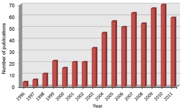
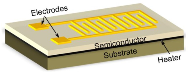
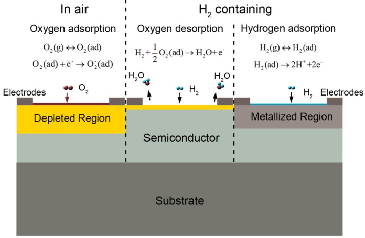
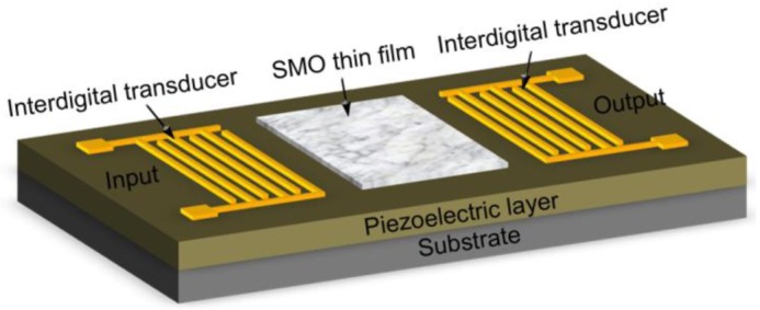
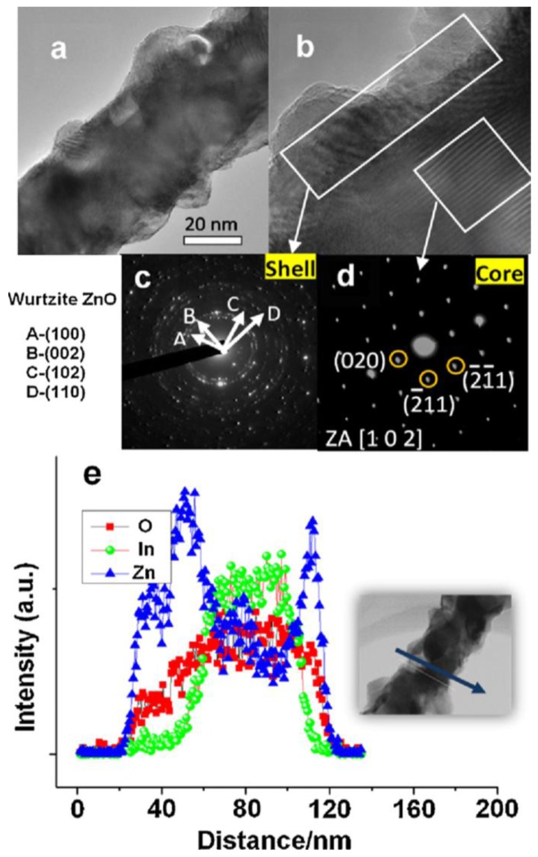
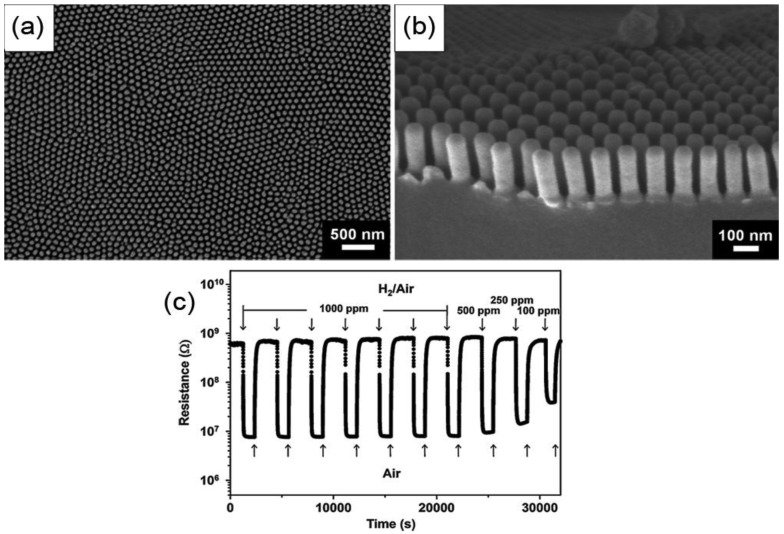
Recently, the hydrogen gas sensing properties of semiconductor oxide (SMO) nanostructures have been widely investigated. In this article, we provide a comprehensive review of the research progress in the last five years concerning hydrogen gas sensors based on SMO thin film and one-dimensional (1D) nanostructures. The hydrogen sensing mechanism of SMO nanostructures and some critical issues are discussed. Doping, noble metal-decoration, heterojunctions and size reduction have been investigated and proved to be effective methods for improving the sensing performance of SMO thin films and 1D nanostructures. The effect on the hydrogen response of SMO thin films and 1D nanostructures of grain boundary and crystal orientation, as well as the sensor architecture, including electrode size and nanojunctions have also been studied. Finally, we also discuss some challenges for the future applications of SMO nanostructured hydrogen sensors.

Keywords: hydrogen gas sensor; nanostructure; one-dimensional nanostructures; semiconductor oxides; thin films.


Figures

Figure 1.
Figure 1.
Publications about semiconductor hydrogen sensors since 1996 according to an enquiry in Thomson Reuters ISI Web of Knowledge.
Figure 2.
Figure 2.
Schematic of a resistance based SMO hydrogen sensor.
Figure 3.
Figure 3.
The hydrogen sensing mechanism of resistance based SMO sensors.
Figure 4.
Figure 4.
The schematic diagram of work function based SMO hydrogen sensors. (a) Schottky diode type; (b) MOS capacitor type; (c) MOSFET type.
Figure 5.
Figure 5.
The schematic diagram of a SAW hydrogen sensor.
Figure 6.
Figure 6.
The resistance changes of sol-gel derived SnO2 thin film sensor during long-term exposure in hydrogen containing environment at 150 °C (reprinted from [66] with permission from Elsevier)
Figure 7.
Figure 7.
The RT hydrogen sensing properties of Nb2O5 NW thin films. (a) Schematic diagram; (b) response to 2,000 ppm of hydrogen in air; (c) hydrogen concentration dependent response; (d) selective response against CO (reprinted from [69] with permission from Elsevier).
Figure 8.
Figure 8.
The response-and-recovery behaviors of CuO thin film oxidized at 400 °C in different dilution gases of (a) dry air and (b) nitrogen at 250 °C (reprinted from [72] with permission from Elsevier).
Figure 9.
Figure 9.
The temperature dependent sensitivity to 1,300 ppm of hydrogen gas in air of Pd/WO3 thin film (reprinted from [78] with permission from Elsevier).
Figure 10.
Figure 10.
The SEM image of dispersed (a) and connect ZnO NWs with 200 nm (b) and 100 nm (c) in diameter; (d) Transient response of the 100 nm ZnO NW-based sensor to 100 ppm of H2 gas at RT (22 °C) (reprinted from reference [96] with permission from Elsevier).
Figure 11.
Figure 11.
(a) SEM image of an individual VO2 NW device with appropriate Ohmic contacts (b) SEM image of a Pd-decorated VO2 NW; (c) I-V curves obtained at 50 °C for Pd-decorated VO2 NW after various exposure times to hydrogen gas (5 sccm), added to the background argon stream (10 sccm); (d) The change in current for a Pd-decorated VO2 NW biased at 10 V as a function of time of exposure to hydrogen gas (reprinted from [99] with permission from The American Chemical Society).
Figure 12.
Figure 12.
The SEM and TEM images of the as-fabricated SnO2 NW gas sensor. low magnifying (a) and high magnifying (b) SEM images; (c) SEM image of the interspace of electrodes; (d) the HRTEM image of one SnO2 NW and the corresponding SAD pattern (inset) (reprinted from [100] with permission from The American Chemical Society).
Figure 13.
Figure 13.
Schematic illustration of the ceramic-tube gas sensor with nanofibers coating on the surface (reprinted from [112] with permission from Elsevier).
Figure 14.
Figure 14.
The TEM analysis of In2O3-ZnO core shell NW. (a) low magnifying TEM image; (b) HRTEM image; (c) SAED pattern obtained from the shell; (d) SAED pattern obtained from the core; (e) line profile obtained by TEM-EDS analysis (reprinted from [116] with permission from Elsevier).
Figure 15.
Figure 15.
The SEM image (a,b) and hydrogen sensing performance (c) of vertically aligned anatase TiO2 nanotube arrays (reprinted from [12] with permission from Elsevier).

References

    1. Hübert T., Boon-Brett L., Black G., Banach U. Hydrogen sensors—A review. Sens. Actuat. B. 2011;157:329–352.
    1. Buttner W.J., Post M.B., Burgess R., Rivkin C. An overview of hydrogen safety sensors and requirements. Int. J. Hydrog. Energy. 2011;36:2462–2470.
    1. Aroutiounian V. Hydrogen detectors. Int. Sci. J. Altern. Energy Ecol. 2005;3:21–31.
    1. Wright J.S., Lim W., Norton D.P., Pearton S.J., Ren F., Johnson J.L., Ural A. Nitride and oxide semiconductor nanostructured hydrogen gas sensors. Semicond. Sci. Technol. 2010 doi: 10.1088/0268-1242/25/2/024002. - DOI
    1. Wang C., Yin L., Zhang L., Xiang D., Gao R. Metal oxide gas sensors: Sensitivity and influencing factors. Sensors. 2010;10:2088–2106. - PMC - PubMed

LinkOut - more resources