

Review
doi: 10.1088/0034-4885/75/3/036501.
Epub 2012 Feb 13.
Engineering metallic nanostructures for plasmonics and nanophotonics
Affiliations
- PMID: 22790420
- PMCID: PMC3396886
- DOI: 10.1088/0034-4885/75/3/036501
Item in Clipboard
Review
Engineering metallic nanostructures for plasmonics and nanophotonics
Rep Prog Phys.
2012 Mar.
Abstract
Metallic nanostructures now play an important role in many applications. In particular, for the emerging fields of plasmonics and nanophotonics, the ability to engineer metals on nanometric scales allows the development of new devices and the study of exciting physics. This review focuses on top-down nanofabrication techniques for engineering metallic nanostructures, along with computational and experimental characterization techniques. A variety of current and emerging applications are also covered.
Figures

Various metallic nanostructures. (a) Periodic nanohole arrays, period 600 nm, in a metallic film exhibit extraordinary optical transmission effects (Ebbesen et al., 1998). Picture used with permission, Elsevier Publishing, from (Krishnan et al.) (b) Metallic bull’s eye structure for channeling light from the concentric rings into the central, subwavelength aperture. The groove periodicity is 500 nm. From (Lezec et al., 2002) Reprinted with permission from AAAS. (c) Silver grating structure with 500 nm periodicity. (d) A sharp metallic tip can concentrate light below the diffraction limit. Image courtesy Lukas Novotny. Used with permission (www.nano-optics.org ). (e) Metal-insulator-metal nanogap plasmon cavity. Scale bar 500 nm. Inset: the 3.3 nm insulating layer. Scale bar 20 nm. Reprinted figure with permission from (Miyazaki and Kurokawa, 2006). Copyright 2006 by the American Physical Society.

(a) Combined with state-of-the-art nanofabrication (<100 nm resolution), nanoplasmonics promises to break the diffraction limit (~ 0.5 µm) at optical frequencies. From (Brongersma and Shalaev, 2010) Reprinted with permission from AAAS. (b) An SPP is an oscillation of the conduction electrons that propagates along the surface of a metal. These hybrid electron-photon waves can be generated and manipulated with metallic nanostructures.

(a) Real part and (b) imaginary part of the complex dielectric functions for Al (Rakić, 1995), Cu (Palik, 1985), Au (Johnson and Christy, 1972), and Ag (Johnson and Christy, 1972). For plasmonic applications, the real part must be negative. For low loss operation, the imaginary part must be small.

(a) Real part and (b) imaginary part of the complex dielectric functions for W (Palik, 1985), Mo (Palik, 1985), and Ta (Weaver, 1974) in the IR range.

(a) A silicon transistor in the 65-nm generation IC technology (Tyagi, 2005). Image courtesy Intel. Reprinted with permission. (b) A silicon transistor in the 45-nm generation IC technology: Gate insulator is grown by atomic layer deposition, followed by a deposition of a metal gate (Mistry, 2007). Image courtesy Intel. Reprinted with permission. (c) Cut-away image showing metal vias. Image courtesy IBM. Reprinted with permission. (d) Multi-layer copper interconnect lines are patterned using a technique known as “damascene”—a combination of copper electroplating followed by chemical-mechanical polishing. Image courtesy IBM. Reprinted with permission.

Lithographic patterning: Option 1: If the substrate is amenable to dry etching (e.g. Si or SiO2), the pattern in the photoresist is readily transferred. Option 2: If the substrate is not amenable to dry etching like most metallic films, a lift-off process is used instead.

(a) Interference lithography can be used to create large-area periodic structures, as shown in the photograph. Reprinted by permission from Macmillan Publishers Ltd: Nature Nanotechnology, (Henzie et al., 2007), copyright 2007. (b) Two interfering coherent beams will generate standing waves to expose the resist. (c) Scanning electron micrograph (SEM) of a 234 nm line pattern in a SiO2 mask on Si. The Si has been partially etched. Image courtesy Ning Cao and Brian Thibeault at the University of California at Santa Barbara Nanofabrication Facility and the National Nanotechnology Infrastructure Network (NNIN). Reprinted with permission.

SEM of the text of Feynman’s 1959 speech (Feynman) in hydrogen silsesquioxane resist, written with a high-resolution e-beam lithography system. Images courtesy Bryan Cord at the University of Minnesota Nanofabrication Center.

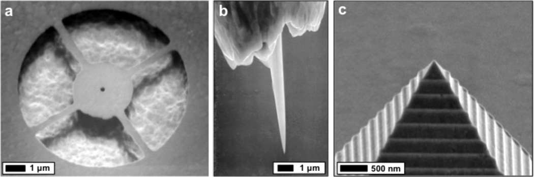
(a) Crystal plane orientation. Pyramidal divots with a tip angle of 70.6 are produced with anisotropic KOH etching of a crystalline silicon wafer. (b) SEM of sharp inverted wedges in a silicon wafer. From (Nagpal et al., 2009). Reprinted with permission from AAAS. (c) Small Au-Ni bilayer pyramid structures released from the silicon mold. Reprinted with permission from (Henzie et al., 2005) Copyright 2005 American Chemical Society. (d) Template stripping (section 2.10) of an upright silver pyramid. From (Nagpal et al., 2009). Reprinted with permission from AAAS.

(a) Schematic showing the similarities and differences between typical e-beam and FIB systems. (b) Schematic of the gallium liquid metal source.

The crystal orientation of a sample can affect the FIB sputtering rates, shown in (a) and (b). (c) The sputtering rate is also affected by the mass of the atoms (orange atoms are more massive), and (d) by the local geometry of the sample. Figure from (Volkert and Minor, 2007) Reprinted with the permission of Cambridge University Press. Copyright 2007.
(a) Single nanohole in a suspended 200 nm thick Ag circular pad. The underlying SiO2 was etched after patterning the Ag via FIB. (b) SEM image of a sharp gold tip fabricated by FIB milling. Image courtesy of Lukas Novotny, from www.nano-optics.org . (c) A silver pyramid with integrated gratings. The gratings were patterned into a KOH-etched silicon mold via FIB and the mold was then used for template stripping (section 2.10). Reprinted with permission from (Lindquist et al., 2010). Copyright 2010 American Chemical Society.

Various soft lithography techniques. (a) replica molding, (b) microcontact printing, (c) micromolding in capillaries, and (d) microtransfer printing.

(a) Illustration of the stencil lithography process. Reprinted with permission from (Vazquez-Mena et al., 2008) Copyright 2008 American Chemical Society. (b) Silicon nitride membranes with 50-nm nanoholes. Image is taken after Pt deposition, showing some clogging. (c) Resultant Pt stencil patterns on the substrate. Panels (b) and (c) Reprinted with permission from (Yan et al., 2005) Copyright 2008 American Chemical Society.

A wide variety of patterned metal nanostructures and 3-D stacks can be fabricated using pattern transfer of thin gold layers from molds followed by cold welding with another gold layer or self-assembled monolayer. The 3-D structure shown in figure (c) is difficult to fabricate by other means. Reprinted with permission of John Wiley & Sons, Inc., Copyright 2004, from (Jeon et al., 2004)

(a) SEM of an alumina-coated silver nanosphere array. Reprinted with permission from (Zhang, 2006) Copyright 2006 American Chemical Society. Only two ALD cycles were used to deposit a sub-1-nm thick film. (b) Cross-sectional image of a gold nanohole array film after encapsulation with ALD silica. Inset: The top surface and vertical sidewall of each nanohole is uniformly coated with 20-nm-thick silica (Im, 2010c). Reproduced by permission of The Royal Society of Chemistry. (c) Vertical nanogap array with a 7-nm gap size fabricated using ALD-grown alumina. Inset: zoomed view showing the 7-nm-gap around the circumference. Reprinted with permission from (Im, 2010a) Copyright 2010 American Chemical Society.

(a) Top-view and (b) zoomed in SEMs of a bull's eye pattern milled into an as-deposited silver film via FIB. The graininess of the pattern is evident. (c) Top-view FIB image and (d) side-view SEM of a bull's eye pattern milled into an ultrasmooth template-stripped silver film. Though the surface is smooth, patterning via FIB still exposes the grains, leading to pattern roughness and degrading the optical performance of the device.

By micro-welding via a platinum gas-injection-system (GIS) inside a FIB chamber, it is possible to perform in situ template stripping of a 200-nm-thick Ag film with a sharp tungsten probe. The smooth underlying silicon surface is clearly seen. Both (a) unpatterned and (b) patterned films can be peeled out (Lindquist et al., 2011).

Template stripping takes advantage of the poor adhesion and good wettability of noble metals on silicon. The top, as-deposited side of the metal films remain rough, but when the film is stripped from the template, the ultrasmooth, patterned interface is exposed. SEMs from Nagpal, et al.(Nagpal et al., 2009) Reprinted with permission from AAAS.

Template stripping of patterned surfaces. (a) An array of silver bumps from a FIB-patterned Si template. From (Nagpal, 2009) Reprinted with permission from AAAS. (b) Multilayer structures, here with silver and alumina, are also possible. From (Nagpal, 2009) Reprinted with permission from AAAS. (c) An array of periodic nanoholes in an optically thick Ag film, still on the silicon mold. Since the deposited film is discontinuous, nanoholes are formed. Reprinted with permission from (Im, 2011) Copyright 2011 American Chemical Society. (d) Patterned silver pyramid made from a Si template etched with KOH and patterned via FIB milling. Reprinted with permission from (Lindquist, 2010) Copyright 2010 American Chemical Society.

Sample FDTD calculation of a single metallic groove. (a) A groove in a metal film will scatter incident light into many channels, both propagative and evanescent. The long-range persistent evanescent wave is an SPP. (b) Monitoring the electric field a distance of 5 µm from the center of the groove with 600 nm plane-wave illumination shows that, for a groove width of 100 nm, the optimal coupling efficiency occurs for a groove depth of 65 nm. (c) A snapshot of the scattered field amplitude at the optimal coupling efficiency. The full electromagnetic field is computed in an FDTD simulation, which includes the incident wave and all scattered waves. For clarity, it is often convenient to subtract the field generated in the absence of the groove, giving only the field scattered by the groove itself. For this simple case, the electromagnetic fields are fully described with a 2-D transverse-magnetic FDTD simulation. Figure from (Lindquist, 2010).

Simulated EOT spectrum. (a) Schematic and (b) FDTD transmission spectrum for a simple EOT test case. The suspended silver film is 100 nm thick, and is perforated with 200 nm diameter holes spaced by 600 nm. Periodic boundary conditions were used in x and y, and the xyz grid size was 4×4×4 nm in and around the area of the holes and Ag film and 4×4×10 nm in free space. PML boundary conditions absorbed all reflected and transmitted light in the ±z directions. A time-pulsed plane-wave was incident from the topside, and the transmitted power was Fourier transformed to calculate the transmission spectrum in a single simulation run. The locations of Wood's anomaly λWood = a = 600 nm, the transmission minimum at 625 nm which corresponds closely with λSPP = 622 nm, and the transmission maximum λpeak at 678 nm are all marked with dashed lines. The peaks are also labeled with the (m,n) grating orders and interfaces on which they occur. Figures 23 and 24 below show electric field maps at these wavelengths. Figure from (Lindquist, 2010).

Simulated EOT field maps. Continuous plane-wave illumination is incident from the +z direction. The time-averaged amplitude of the z component of the electric field is pictured. (a) λ=600 nm generates a non-resonant Rayleigh-Wood anomaly in which the field is de-localized from the SPPs and is diffracted tangent to the silver film. (b) λ=625 nm corresponds to the transmission minimum. SPPs are excited, but weakly, especially on the bottom side of the film. (c) λ=678 nm corresponds to a transmission maximum. The SPPs are excited symmetrically and are very intense. The field intensities are scaled by 4, 2, and 1 for (a), (b), and (c), respectively, for the same intensity scale bar. The transmission maximum has the most intense SPP fields. Figure from (Lindquist, 2010).

Simulated EOT electric field lines. A snapshot of the total electric field is shown, with field lines overlayed. (a) At a transmission minimum, λ=625 nm, the SPP field lines and inferred charge distributions are anti-symmetric, arising from Fano-type destructive interference between the grating-coupled SPPs and the local excitation of the nanohole. (b) At a transmission maximum, this interference is constructive, building up significant field intensity within the nanoholes and boosting the transmission. The field intensities are scaled by 2 and 1 for (a) and (b), respectively. The transmission maximum has the most intense surface fields. Figure from (Lindquist, 2010).

Two-dimensional FDTD simulation of a slit-groove interferometer. The time-averaged Poynting vector is plotted on a log scale. A fraction of the SPPs that propagate from the slit to the groove are scattered into far-field radiation, and are detectable with an imaging spectrometer. Figure from (Lindquist, 2010).

Propagation length measurements with a slit-groove interferometer. (a) SEM of a single slit and a single groove milled with FIB through a 200 nm thick Ag film. (b) Propagation length measurements. The diamonds show ltot measured from a template-stripped 200 nm thick silver film. The solid line depicts lohm calculated from ellipsometry data. Control measurements were also made on a rough as-deposited film for comparison (dots), along with previously reported data (squares)(van Wijngaarden, 2006). From (Nagpal, 2009) Reprinted with permission from AAAS.
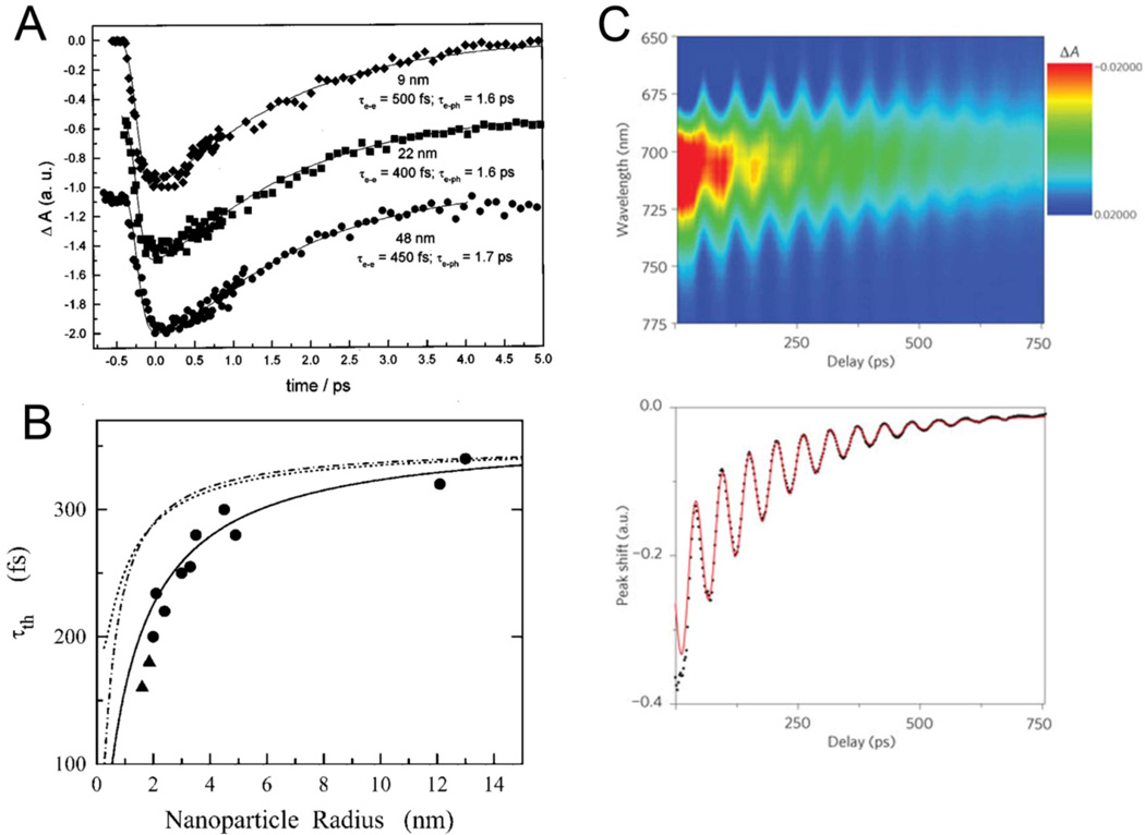
(a) Time-resolved transient absorption measurements on different sized metal nanospheres showing identical electron relaxation dynamics Reprinted with permission from (Link and El-Sayed, 1999). Copyright (1999) American Chemical Society. (b) Electron thermalization time for small silver nanospheres showing identical (~310 fs) relaxation times for large particles (>5 nm), but a sharp decrease in thermalization time for nanoparticles between 2–5 nm (Voisin, 2000). Reprinted figure with permission from (Voisin, 2000) Copyright (2000) by the American Physical Society. (c) Coherent acoustic phonon oscillations launched due to a sharp increase in lattice temperature following electron-phonon cooling. The oscillation period strongly depends on mechanical properties of metal nanoparticle and surrounding media (Pelton, 2009). Reprinted by permission from Macmillan Publishers Ltd: Nature Nanotechnology (Pelton, 2009), copyright (2009).

Aperture probes and apertureless probes for NSOM. (a) SEM of a 70-nm aperture surrounded on all sides by 100-nm-thick aluminum. From (Betzig and Trautman) Reprinted with permission from AAAS. (b) A pulled fiber tip carrying a single gold nanoparticle used for apertureless NSOM. Reprinted figure with permission from (Kuhn et al.) Copyright 2006 by the American Physical Society. (c) SEM showing a gold particle attached to the end of an optical fiber. Reprinted figure with permission from (Anger et al.) Copyright 2006 by the American Physical Society (d) SEM of an asymmetrical gold tip made with FIB. Reprinted figure with permission from (Sanchez et al.) Copyright 1999 by the American Physical Society. (e) SEM of an aluminum nano-antenna sculpted with FIB. Reprinted by permission from Macmillan Publishers Ltd: Nature Photonics, (Taminiau et al.), copyright 2008. (f) SEM of a conical metallic tip with a grating SPP coupler made by FIB. Reprinted with permission from (Ropers et al.) Copyright 2007 American Chemical Society.
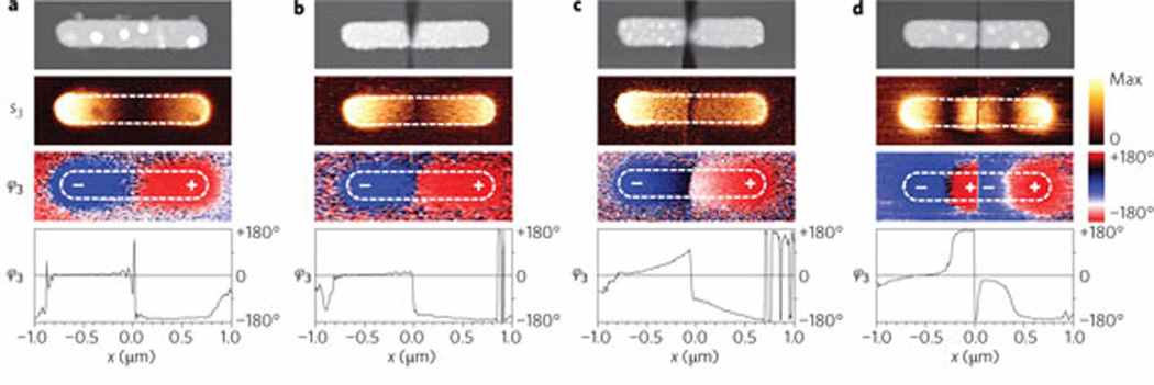
Phase-resolved near-field intensity measurements that map nanowire antennas, with gaps of increasing separation in the middle. In each panel, the top image shows the topography, the middle image shows the near-field light amplitude, and the lower image shows the phase of the scattered light collected using a silicon apertureless NSOM. Finally, the bottom graphs plot high-resolution electric-field intensity maps, which show optical hot spots and experimentally confirm the plasmon modes expected in the antennas. Reprinted by permission from Macmillan Publishers Ltd: Nature Photonics, (Schnell, 2009), copyright 2009.

(Left) Scanning electron micrographs of a 18.6 µm long silver nanowire with diameter of 120 nm. (Right) NSOM image, via PSTM method, shows surface plasmon propagation along the silver nanowire. Reprinted figure with permission from (Ditlbacher et al.) Copyright 2005 by the American Physical Society.
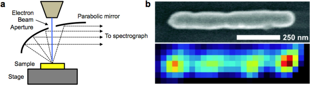
(a) Schematic of a typical CL setup consisting of a parabolic mirror with an aperture. (b) High resolution scans of a metal nanorod imaged with a CL setup. The top image shows the topography, and the bottom image depicts the density of states excited by the fast electrons incident on the metal nanostructure. CL imaging provides correlated topography and plasmonic local density of states excited by the electrons, scanned with high precision. Reprinted with permission from (Vesseur et al., 2007) Copyright 2007 American Chemical Society.

(a) High-resolution EELS scans showing higher-order plasmon modes in silver nanotriangular prisms (Nelayah et al., 2007). (b) STEM-EELS mapping depicts the plasmonic local density of states (LDOS) excited by electrons. The energy of the LDOS is measured by the energy loss and the spatial distribution is mapped by the EELS image after removal of the zero-loss peak (Nelayah et al., 2009). (c) LDOS depicting plasmonic hot spots in coupled metal nanostructures. Both bright and dark (i.e. nonradiative) plasmon modes can be mapped using EELS (N'Gom et al., 2009).

(a) Schematic depicting the setup used for time-resolved photoemission electron microscopy using different colored beams. (b) Topography of the imaged metal nanostructure. (c–e) PEEM images with different beams and time delays on the pump-probe measurement. The scans show the richness of the data obtained with high resolution in time and space for nanoplasmonic systems (Aeschlimann et al., 2010). (f) PEEM images showing both localized and propagating surface plasmons in metal gratings. (g) Time-resolved measurements showing dephasing of excited state electrons vs. time for surface plasmon polaritons. Reproduced with permission from (Kubo et al., 2007a). Copyright (2007) IOP Publishing, Ltd.

(a) Simulated binding responses with “typical” values of cA (200 nM, 50 nM, 20 nM, and 5 nM), ka (105), and kd (10−3). With such real-time measurements, the on-off rates (kinetics) and affinity of a reaction can be measured. All three parameters (KA, ka, and kd) are important, since two reactions can have the same affinity ka/kd, but have different kinetics. (b) The Langmuir isotherm equation is plotted for receptor-analyte pairs with different KD values (1 pM and 1 nM). As an example, consider a 1 µm × 1 µm sensor chip that is coated with 104 receptor molecules, and assume that KD = 1 nM between the receptor and analyte. If the analyte concentration is 1 pM, Req/Rmax ~10−3 according to Eq. 11, thus only 10 molecules will be bound to the sensor in equilibrium. As this example shows, the kinetics and equilibrium constants guide the design of surface-based affinity biosensors. For further details, see (Squires et al.).
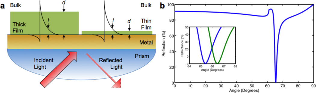
(a) Schematic depicting evanescent SPP waves and their excitation with a prism in a total internal reflection setup. The decay length l of the SPP determines its sensitivity to a film of different thicknesses. When the film thickness d is small compared to l, the SPP will probe the refractive indices of both the film and the bulk solution above the film. (b) Simulated SPR excitation. At the correct angle, SPPs are excited at 850 nm illumination for a 50 nm thick Au film. The inset shows a 1° shift in the SPP resonance dip when the bulk refractive index above the Au film changes from 1.32 to 1.33. This sensitivity of 100 deg/RIU (Refractive Index Unit) is typical for prism-based SPR instruments (Pang et al.).

(a) A periodic array of nanoholes milled through a thin Au film. (b) At resonant wavelengths, the incident light is efficiently transmitted, giving a sharp transmission peak. As molecules bind, the peak shifts, modulating the transmission. (c) Side view: 3-D FDTD simulation of the EOT effect through a nanohole array. Intense optical energy is observed, confined within ~100 nm from the surface. Molecular binding on or near the surface modulates this field distribution, and the optical transmission process, providing the basis for measuring binding events.

(a) EOT peak shifts due to binding of molecules Reprinted with permission from (Brolo et al., 2004) Copyright 2004 American Chemical Society. (b) Sharp apexes in a double-hole aperture enhance the detection sensitivity. Reprinted with permission from (Lesuffleur et al.) Copyright 20047, American Institute of Physics. (c) An array of 3×3 nanoholes occupying ~1 um2 footprint can be used as a sensing element (Lindquist et al.). Image reproduced by permission of Sang-Hyun Oh and The Royal Society of Chemistry from [Lab Chip 9, 382 (2009)]. (d) Multiscale patterning of nanoholes using soft interference lithography. Reprinted by permission from Macmillan Publishers Ltd: Nature Nanotechnology, (Henzie et al.) Copyright 2007.

(a) SPR imaging with nanohole arrays. Reprinted with permission from (Yang, 2008) Copyright 2008 American Chemical Society. (b) Nanohole arrays made with interference lithography with Fano-type lineshapes for SPR sensing in the NIR regime. Reprinted with permission from (Tetz, 2006) Copyright 2006, The Optical Society (OSA).

Membrane biosensing schemes: (a) LSPR sensor has been integrated with lipid membranes by utilizing localized rupture of phospholipid vesicles on silicon dioxide in the bottom of nanometric holes in a thin gold film Reprinted with permission from (Dahlin et al., 2005). Copyright 2005 American Chemical Society. (b) Pore-spanning lipid membrane (nano-black lipid membrane) covering an anodic aluminum oxide (AAO) nanopores. Reprinted with permission from (Lazzara, 2011). Copyright 2011 American Chemical Society. (c) Colorized SEM of a nanopore array made on a suspended Au/Si3N4 membrane. (d) The ability to fill both sides of the membrane with a buffer makes this geometry a unique platform to study transmembrane proteins. From (Im et al., 2010c) Both (c) and (d) reproduced by permission of the Royal Society of Chemistry.

Basic SERS electromagnetic enhancement. A gold nanoparticle will enhance both (a) the incident field, as well as (b) the scattered field, greatly boosting the Raman signal from a proximate molecule. Since the intensity is enhanced twice, i.e. the nanoparticle acts as both a receiver and a transmitter, the SERS signal is proportional to the intensity of the incident field squared.

Plasmonic nanofocusing. (a) Two types of modes exist for an IMI tip. An even-field mode (odd charge distribution) will have zero charge at the tip, and as the SPP travels down the metal taper to the sharp tip, the field distribution resembles that of a wave propagating in the dielectric, and no plasmonic nanofocusing occurs. However, an odd-field mode (even charge distribution) will have large charge density at the tip. The SPPs traveling on either side of the taper will arrive to the tip with their charge distributions in phase. With this mode, the propagating SPP becomes a localized at the tip, focusing its energy into a nanoscale volume. As the tip tapers to a finite size, the resulting high-intensity field is oriented longitudinally, i.e. along the tip axis. (b) Plotting the dispersion of the odd-mode SPP shows that the wavenumber kspp at a given frequency increases with decreasing metal thickness. Once the metal thickness becomes on the order of the skin depth δm, the two SPPs on the top and bottom of the thin metal film will couple. The mode with odd field symmetry will generate the large wavevectors suitable for plasmonic nanofocusing. Figure from (Lindquist, 2010).

SEMs of a (a) symmetrically and (b) asymmetrically patterned silver pyramids produced via template stripping. (c,d) FDTD simulations of the same structures. The asymmetry is necessary to convert linearly polarized light into a longitudinal (along the z-axis) field at the tip. For 710 nm wavelength illumination, the hotspot is calculated to be 28×32×14 nm3. Panels reprinted with permission from (Lindquist, 2010) Copyright 2010 American Chemical Society.

Highly directional emission of photons from a single quantum dot coupled to a metal nanostructure (a Yagi-Uda antenna). The image shows comparisons between the directionality of emission from a reference quantum dot (“Ref”), grating, and directional Yagi-Uda antenna (“YU”) at visible wavelengths. Such high-efficiency coupling of quantum dots with SPPs can potentially be utilized for on-chip generation of single-photon sources for quantum computing. From (Curto et al., 2010) Reprinted with permission from AAAS.

Plasmonic optical data storage. (a) Proposed optical data storage technique, with each bit-cell composed of multiple arrangements of nanobumps or nanoholes. (b) In reflection-mode operation. (c) The data can also be recorded in multiple tracks on a metal film. Scheme adapted from (Mansuripur et al., 2009) Used with permission of The Optical Society (OSA), Copyright 2009.

Demonstration of five-dimensional plasmonic optical recording. The 18 different images are read-out from the same 100-by-100 µm area using two different laser polarizations (indicated by arrows at bottom) and three different wavelengths (indicated on the left). Reprinted by permission from Macmillan Publishers Ltd: Nature, from (Zijlstra et al., 2009), copyright 2009.

(a) A typical thin-film PV structure. (b) Metallic nanoparticles can enhance light-trapping efficiency by increasing optical path lengths within PVs; Since nanoparticles cannot act as electrodes, transparent contacts (e.g. ITO) are needed. (c) LSPR effects using embedded nanoparticles. Used in tandem OPVs etc. Field enhancement is short-range (~10 nm). (d) Replace expensive ITO with ultra-thin metallic films with or without patterning. (e) Patterned metal contact on the backside can launch SPPs and increase optical path lengths. (f) Combined schemes (d) and (e) and potentially utilize coupling between top and bottom electrodes.
References
-
- Achermann M, Shuford KL, Schatz GC, Dahanayaka DH, Bumm LA, Klimov VI. Near-Field Spectroscopy Of Surface Plasmons In Flat Gold Nanoparticles. Optics Letters. 2007;32:2254–2256. - PubMed
-
- Aeschlimann M, Bauer M, Bayer D, Brixner T, De Abajo FJ, Pfeiffer W, Rohmer M, Spindler C, Steeb F. Adaptive Subwavelength Control Of Nano-Optical Fields. Nature. 2007;446:301–304. - PubMed
-
- Ahonen M, Pessa M, Suntola T. Study Of Znte Films Grown On Glass Substrates Using An Atomic Layer Evaporation Method. Thin Solid Films. 1980;65:301–307.
-
- Alcantar NA, Park C, Pan JM, Israelachvili JN. Adhesion And Coalescence Of Ductile Metal Surfaces And Nanoparticles. Acta Materialia. 2003;51:31–47.
Publication types
MeSH terms
Grants and funding
LinkOut - more resources
Full Text Sources
Other Literature Sources