Review
. 2012 Nov 14;24(43):5782-825.
doi: 10.1002/adma.201201482. Epub 2012 Aug 29.

Graphene: an emerging electronic material

Affiliations
Review

Graphene: an emerging electronic material

Nathan O Weiss et al. Adv Mater. .

Abstract

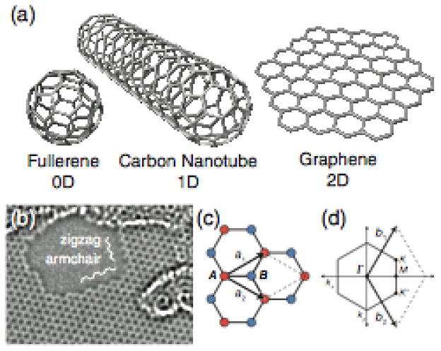
Graphene, a single layer of carbon atoms in a honeycomb lattice, offers a number of fundamentally superior qualities that make it a promising material for a wide range of applications, particularly in electronic devices. Its unique form factor and exceptional physical properties have the potential to enable an entirely new generation of technologies beyond the limits of conventional materials. The extraordinarily high carrier mobility and saturation velocity can enable a fast switching speed for radio-frequency analog circuits. Unadulterated graphene is a semi-metal, incapable of a true off-state, which typically precludes its applications in digital logic electronics without bandgap engineering. The versatility of graphene-based devices goes beyond conventional transistor circuits and includes flexible and transparent electronics, optoelectronics, sensors, electromechanical systems, and energy technologies. Many challenges remain before this relatively new material becomes commercially viable, but laboratory prototypes have already shown the numerous advantages and novel functionality that graphene provides.


Figures

Figure 1
Figure 1. Honeycomb lattice
(a) Allotropes of carbon based on two-dimensional graphene (right): quasi-zero-dimensional buckminsterfullerene (left) and quasi-one-dimensional armchair nanotube (middle). (b) High resolution TEM image of suspended graphene, showing a monolayer with a void in the middle and with a bilayer region toward the top. Clear zigzag and armchair edges are seen. (c) Hexagonal crystal structure of graphene with lattice parameters a1 and a2 and inequivalent atomic positions A and B of the diatomic basis shown in red and blue. (d) Reciprocal lattice and BZ with reciprocal lattice parameters b1 and b2, showing Dirac points K and K′ at the BZ corners, as well as M, the midpoint of the BZ edge and Γ, the center of the BZ. Recreated from[46] (c). Adapted with permission from[496] (b). Copyright: 2009 American Association for the Advancement of Science (b).
Figure 2
Figure 2. Electronic band structure
(a) Band structure of graphene; (b) the linear dispersion relation showing the vertically mirrored Dirac cones intersecting at the Fermi energy, EF. Comparison of band structures of (c) massless Dirac like particles in monolayer graphene (d) massive Dirac particles in bilayer graphene with parabolic shape, (e) a typical direct band gap semiconductor with Schrödinger particles, asymmetric electron-hole effective mass (dissimilar curvature), and a substantial band gap. (f) Opening a band gap, Eg, in monolayer graphene causes a rounding of the Dirac cone tips, and (g) an inverted tip for bilayer graphene. Recreated from[46] (a) and[3,6] (c–g).
Figure 3
Figure 3. Unique and unusual electronic properties
(a) Dirac cones showing pseudospin as it rotates with respect to reciprocal space and the inverted orientation between the two valleys. (b) ARPES map of the pseudospin, horizontal cross section of a Dirac cone observed experimentally using spherically polarized photons. (c) Hall resistance measurements, showing quantized peaks and plateaus. (d) Landau levels for the anomalous and fractional QHE in graphene, with n as the quantum number index of Landau levels, not the carrier concentration. Adapted with permission from[55] (b) and[3] (c). Copyright: 2010 Institute of Physics (b) and 2009 American Association for the Advancement of Science (c).
Figure 4
Figure 4. Field effect transistors
Schematics of (a) a typical back-gated GFET between two source-drain electrodes, with a potential applied to the bottom of the device acting as a global capacitor that modulates energy level of graphene; (b) a dual back- and top-gated device, showing the localized gate capacitor fabricated on top of the channel; (c) a top-gate only device fabricated on EG on an insulating SiC substrate. (d) Schematic of band structure shift as gate voltage dopes graphene above and below the Dirac point. (e) Typical resistivity as a function of gate voltage for graphene, showing the ambiploar nature as conduction switches between the hole (left) and electron (right) regimes, separated by the charge neutrality (Dirac) point where resistance reaches its maximum. (f) Current saturation and switching threshold voltage in a conventional FET. (g) Velocity of charge carriers in graphene as a function of electric field, compared with other semiconductors. Recreated from[6] (a–c) and[3] (e). Adapted with permission from[6] (f and g). Copyright: 2010 Nature Publishing Group (f and g).
Figure 5
Figure 5. Supported and suspended graphene
(a) Electron-hole puddles within graphene samples on a substrate measured through STS. Surface roughness via STM topography images for graphene on SiO2 (b) and hBN (c) showing the ultraflat hBN surface. (d) False color SEM image of suspended graphene sample (red) between to electrodes (yellow) used to reduce substrate effects such as scattering and improve mobility. (e) Ripples in an annealed, suspended sample. Adapted with permission from[109] (a),[119] (b and c),[64] (d) and[132] (e). Copyright: 2007 (a), 2009 (e) and 2011 (b–d) Nature Publishing Group.
Figure 6
Figure 6. Synthesis techniques
(a) Optical microscopy image of a very large micromechanically exfoliated (tape method) monolayer of graphene. Note the considerable contrast for the single atomic layer. (b) Photograph of dispersed graphene by ultrasonic exfoliation of graphite in chloroform and (c) deposited on a bendable film. (d) Graphene oxide and reduced graphene oxide showing the remaining oxygen rich functional groups after reduction. (e) OM and (f) SEM images of graphene grown epitaxialy on SiC. Number of layers is shown in (f), with multiple layers forming at step edges. (g) Crystal structure of 4H-SiC with Si (top) and C (bottom) faces. (h) False colored dark field TEM reconstruction of CVD graphene domain patchwork. Each color is a domain with a certain lattice orientation (left), imaged separately using the corresponding diffracted beams for crystal orientation dependent contrast (right). (i) High resolution ADF-STEM of a domain boundary in CVD graphene showing a rotational mismatch of 27° and a series of pentagon-heptagon pairs (Stone-Wales defects) along the boundary. (j) SEM of an array of seeded growth hexagonal domains of CVD graphene on copper. (k) Large area graphene transferred using roll-to-roll production spanning 30 inches diagonally. (l) Schematic of the roll-to-roll process showing adhesion to a thermal release tape polymer support, run through an etching medium to remove the copper foil, before being released via heat treatment from the polymer support onto the final substrate. Recreated from[336] (g). Reproduced with permission from[4] (a–c),[219] (d),[89] (e and f),[274] (h and i),[275] (j) and[364] (k and l). Copyright: 2009 American Association for the Advancement of Science (a–c), 2011 Springer (d), 2010 Cambridge University Press (g), and 2009 (e and f), 2010 (k and l), and 2011 (h–j) Nature Publishing Group.
Figure 7
Figure 7. Raman spectroscopical characterization
Schematic band diagrams of Raman resonance pathways for (a) G, (b) D, (c) D′, and (d) double resonance 2D (G′) peaks of monolayer graphene. (e) Raman spectroscopy of pristine (upper left) and at an edge (lower left) of a monolayer, showing D, G, D′ and 2D (G′) peak heights and 2D peaks of 1 through 4 layers and bulk graphite (right), showing the broadened FWHM and multi-peak fits for multilayers. Recreated and adapted with permission from.[319] Copyright: 2009 Elsevier.
Figure 8
Figure 8. Metallic components
Transmittance vs. wavelength compared to other TCs (a). (b) Transmittance vs. sheet resistance of graphene (solid shapes) and other materials (hollow triangles). The lowest sheet resistance graphene samples are CVD graphene (blue triangles)[364] and FeCl3 intercalated, ME few-layer graphene (black diamonds).[340] Device schematic (c) and performance (d) of a graphene based LCD. (e) A light-emitting electrochemical cell, using graphene and poly(3,4-ethylenedioxythiophene) (PEDOT) as transparent electrodes and n-/p-doped Super Yellow (SY) polymer as the active emitter, with a photographic of the transparent cell bent around a secondary red light (f). (g) Photograph of a CVD graphene based resistive touch screen. (g) A dye-sensitized solar cell with graphene TC. (h) An ultracapacitor unit cell using two stacked CMG electrodes with a porous spacer impregnated by electrolyte, sandwiched by metal foil current collectors and encapsulated (not shown) by a steel and Mylar test structure. Recreated from[376] (a),[340,376] (b),[375] (c),[383] (e),[238] (g), and[421] (i). Adapted with permission from[375] (d),[383] (f) and[364] (g). Copyright: 2008 (d) and 2010 (f) American Chemical Society and 2010 Nature Publishing Group (g)
Figure 9
Figure 9. Radio frequency top-gated devices
(a) Photograph and (b) SEM false color image of two EG on SiC FETs patterned on the surface; (c) schematic, (d) SEM image with cross section (inset) of a self-aligned nanowire-gated (SANW) device. (e) Current gain vs. frequency for EG as well as SANW gated devices of peeled and CVD graphene. The cutoff frequency is the extrapolated intersection of the 1/f trend line with a current gain |h21|of one. Gate length dependence of transit time and drift velocity, vDrift, of short channel self-aligned devices (f). (g) Comparison of cutoff frequency and channel length of high mobility materials. Hollow circles are for bulk semiconductors: silicon based metal-oxide semiconductor FET (MOSFET) (light blue) and GaAs and InP HEMTs (light green and light red), and the black circles are for carbon nanotube based devices, all adapted from.[6] Micromechanically exfoliated/peeled (ME) graphene (squares),[459,460,475] CVD graphene (diamonds)[470,471] and epitaxial graphene on SiC (orange triangles).[,–466] Self-aligned nanowire-gated device with ME (navy blue squares)[149] and CVD (navy blue diamond)[454] as well as projected cutoff frequencies (pink stars)[453] are shown. Recreated from[149] (c),[149,453,454,463,464,466,470] (e),[453] (f) and[6,149,453,454,463,464,466,470] (g). Adapted with permission from[463] (a and b),[149,454] (d). Copyright: 2009 American Association for the Advancement of Science (a and b), 2011 American Chemical Society (d and f) and 2010 Nature Publishing Group (g)
Figure 10
Figure 10. Integrated Circuits
Circuit design for a GFET based frequency double (a) and mixer (d). (b) Oscilloscope readout (b) of input (top) and output (bottom). Frequency spectrum (c) of the frequency doubler. (e) Schematic of a frequency mixer device and components. (f) Optical micrograph of the fabricated device on a SiC substrate. (g) Output frequency spectrum of the mixer. Recreated from[479] (e). Adapted with permission from[454] (a–c) and[479] (d, f, and g). Copyright: 2011 American Chemical Society (a–c) and 2011 Nature Publishing Group (d, f, and g).
Figure 11
Figure 11. Nanostructures
(a) Nanoconstriction (b) quantum dot/point contact SET and (c) GNRs of varying width, patterned using EBL and imaged using SEM. (d) AFM topography of sonicated GNRs of width ~50 nm, ~20 nm, and ~10 nm from left to right; the narrowest GNR is two layers thick. (e) STM topography of the curled edge of a CNT-derived ribbon deposited on metal. (f) STM topography of GNRs with atomically smooth edges: 10 nm × 120 nm straight (top) and 8-nm-wide with a 30° kink (bottom). Schematics of GNRs fabricated with a nanowire mask (g) and nanowire top-gate (h), with SEM cross section of the latter (i). EG nanoribbons grown on a prepatterned, nanofaceted SiC (11̄0n) crystal surface (j), device schematic (k). (l) AFM topography of trenches on a SiC substrate (top) and post growth semicircular plateaus with a sub-40-nm GNR along the nanofacet. (m) Schematic and (n) TEM image of a graphene nanomesh patterned using block copolymer based lithography. Recreated from[533] (g),[115] (h),[93] (j and k), and[512] (m). Adapted with permission from[515] (a),[483] (b),[490] (c),[503] (d),[501] (e),[506] (f),[115] (i),[93] (l) and[512] (n). Copyright: 2008 American Association for the Advancement of Science (b and d), 2007 Elsevier (c), 2011 (f) and 2010 (l and m) Nature Publishing Group and 2010 American Chemical Society (i).
Figure 12
Figure 12. Band gap engineering
(a) Energy-gap vs. width, (b) mobility vs. ribbon width, and (c) band gap vs. ribbon width. (d) Substrate induced band gap in EG on SiC, measured by ARPES. (e) FET band schematic: as the source drain bias overcomes the band gap, current will begin to flow. Applying a gate voltage will shift the cones and gap up and down, aligning the source-drain Fermi levels with the valence and conduction bands respectively where current will then flow. (f) GNR band structure schematic and potential puddles, demonstrating an enhanced transport gap. (g) Two-dimensional electron transport plot of conductance vs. gate and bias voltages showing Coulomb diamond of a GNR. The height of the diamond represents the effective band gap (h) SET Coulomb diamonds; the height of the diamonds represents the transport gap. (inset) Dependence of the diamond widths on the diameter of the quantum dot islands. (i) Current ratio of GNR magnetoresistance I(8 T)/I(0 T) as a function of gate and bias voltages, showing the large increase in current with application magnetic field. Recreated from[6,93,115,524,533] (a–c) and[485] (e). Adapted with permission from[94] (d),[519] (f), [485] (g),[483] (h) and[533] (i). Copyright: 2010 (i) 2007 (d) Nature Publishing Group, 2007 (g) and 2010 (f) American Physical Society, and 2008 American Association for the Advancement of Science (h).
Figure 13
Figure 13. Stacked Graphene
(a) Stacking order of rhombohedral (ABCA) and Bernal (ABAB) varieties. (b) Dirac point tunability and increased on/off ratio of dual-gated bilayer graphene. Band gap dependence on the applied vertical field, shown as a function of the average displacement field in bilayer graphene (c) and as a function of charge density in trilayer graphene (d), with comparisons to theoretical models. Adapted with permission from[540] (b and c) and[547] (d). Copyright: 2009 (b and c) and 2011 (d) Nature Publishing Group.
Figure 14
Figure 14. Strain Engineering
(a) Schematic diagram of strain induced shifting of the Dirac cones. (b) A region of uniaxial strained graphene separates two unstrained regions, creating a transport gap between the two misaligned Dirac cones. (c) Overlapping cones showing regions of possible states through a barrier of uniaxially strained graphene. 1) Scattering states, 2) band states within the strained region, 3) localized states at boundary, 4) filtered states, and 5) filtered, evanescent waves. (d) The resonant bands between the unstrained and strained region, and surface modes that appear at the junction, similar to the edge states of a nanoribbon. (e) Triangularly symmetric strain profile that produce gauge fields and in turn pseudomagnetic effects in graphene. (f) Band structure showing the opposite direction of the pseudomagnetic field on each sublattice point, with quantized Landau levels, and no net field. (g) STM topography of a highly strained graphene nanobubble, and (h) STS of the Landau levels of the observed pseudomagnetic field in experimentally produced nanobubbles. (i) Microcapsule sealed by suspended graphene that forms a bubble due to pressure differentials. (j) False color SEM images of a graphene device suspended over a trench that is then strained into the trench using an in situ nanoindenter with electromechanically coupled measurements. Recreated from[49] (b–d) and[156] (e). Adapted with permission from[157] (g and h),[39] (i) and [552] (j).[559] Copyright: 2010 American Association for the Advancement of Science (g and h), 2011 Nature Publishing Group (i) and 2010 American Chemical Society (h).
Figure 15
Figure 15. Spintronics
(a) Half-metallicity of ZGNRs. DOS schematics show a polarized spin at the edges (left). With an in-plane electric field applied, the DOS shifts to remove the band gap (right). (b) SEM and (c) schematic of four-terminal spin injection measurements. (d) Schematic of the diffusion and precession of spin polarized currents in the four-terminal device when electrode magnetization is aligned parallel or antiparallel. (e) Schematic of a proposed valley valve using perpendicular electric fields applied to bilayer graphene to polarize pseudospin. Recreated from[486] (a). Adapted with permission from[153] (b–d) and[582] (e). Copyright: 2007 Nature Publishing Group (b–d) and 2009 American Physical Society (e).
Figure 16
Figure 16. Photodetectors
(a) Energy band schematic of the broadband absorption of light by graphene. (b) Photocurrent measurements of a graphene photodetector over the whole channel by SPCM. The results clearly show the anti-symmetric photocurrent at source electrode and drain electrode, while nearly zero photocurrent is observed at the middle of the device channel; (c) Band profile of the graphene photodetector. ΔϕTi represents the difference between the Dirac point energy and Fermi level in Ti-doped graphene. The titanium electrode contact slightly dopes the graphene with electrons to shift its Fermi level up towards the Dirac point, and creates a potential barrier between the graphene under the electrodes and within the channel; (d) The photocurrent measure at different gate voltages (form 40 V to 60 V). The results indicate that both increasing or decreasing the gate voltage from 15 V will enlarge the peak amplititude and shift the peak position toward the electrode; (e) High frequency measurements, which show the device performs well up to 40 GHz. The inset pictures the photoresponsivity at different gate voltage both for DC measurements or high frequency AC measurements; (f) The schematics of the antisymmetric design to break the band mirror. The multi-finger design enlarges the photoresponsivity. (g) False color SEM image of a real multi-finger photodetector. Recreated from[598] (f). Adapted with permission from[143] (b),[594] (c),[596] (d),[152] (e),[598] (g). Copyright: 2008 (b), 2011 (c), 2009 (e) and 2010 (f) Nature Publishing Group and 2009 American Chemical Society (d).
Figure 17
Figure 17. Manipulating light waves
(a) Schematic showing the components in a graphene based mode-locked laser system; (b) The oscilloscope data show the graphene based mode-locked laser can perform at ultrafast speeds; (c) The SEM image of a graphene optical modulator structure; (d) High frequency measurement of device response as a function of frequency. The 3 dB bandwidth results are around 1 GHz with different gate voltage at −2 V, −2.5 V, −3 V, −4 V; (e) Schematics of graphene based polarize with graphene easily coupled in the self-polished optical fiber; (f) Optical intensity at different polarized angles. Adapted with permission from[599] (a),[600] (b),[601] (c and d) and[602] (e and f). Copyright: 2010 American Chemical Society (b) and 2011 Nature Publishing Group (c–f).
Figure 18
Figure 18. Sensors
(a) Schematic of a GFET based sensor, showing solution making contact with the graphene channel, and a reference electrode. (b) Carrier concentration changes, Δn, of graphene as a function of the concentration of the exposed NO2 source. (Upper inset) False color SEM of the Hall bar device. (Lower inset) Field effect characterization of the device. (c) Changes in resistivity, ρ, at zero magnetic field, B, caused by graphene’s exposure to various gases diluted in concentration to 1 ppm. (d) Observation of changes in the Hall resistivity near the Dirac point during adsorption (blue) and desorption (red) of diluted NO2 and reference curve (green). (e and f) Statistical distribution of step heights (e) without its exposure to and (f) during a slow desorption of NO2. Adapted with permission from[619] (b–f). Copyright: 2007 Nature Publishing Group.
Figure 19
Figure 19. M/NEMS
Graphene nanoresonator, suspended over a trench: schematic (a) and false color SEM (b). Rippled graphene on a prestrained PDMS substrate, up to 30% strain: (c) schematic of the device, and (d) AFM of the periodically buckled ripples along the graphene strips on the relaxed substrate.. Recreated from[651] (a) and[557] (c). Adapted with permission from[644] (b) and[557] (d). Copyright: 2007 American Association for the Advancement of Science (b) and 2011 American Chemical Society (d).

Similar articles

Cited by

References

    1. Novoselov KS, Geim AK, Morozov S, Jiang D, Zhang Y, Dubonos SV, Grigorieva IV, Firsov AA. Science. 2004;306:666. - PubMed
    1. Novoselov K, Geim A, Morozov S, Jiang D, Katsnelson M, Grigorieva I, Dubonos S, Firsov A. Nature. 2005;438:197. - PubMed
    1. Geim AK, Novoselov KS. Nat Mater. 2007;6:183. - PubMed
    1. Geim AK. Science. 2009;324:1530. - PubMed
    1. Moore GE. Electronics. 1965;38:114.

Publication types

LinkOut - more resources