. 2012 Oct 5;23(39):395705.
doi: 10.1088/0957-4484/23/39/395705. Epub 2012 Sep 12.

An investigation into the feasibility of myoglobin-based single-electron transistors

Affiliations

An investigation into the feasibility of myoglobin-based single-electron transistors

Debin Li et al. Nanotechnology. .

Abstract

Myoglobin single-electron transistors were investigated using nanometer-gap platinum electrodes fabricated by electromigration at cryogenic temperatures. Apomyoglobin (myoglobin without the heme group) was used as a reference. The results suggest single-electron transport is mediated by resonant tunneling with the electronic and vibrational levels of the heme group in a single protein. They also represent a proof-of-principle that proteins with redox centers across nanometer-gap electrodes can be utilized to fabricate single-electron transistors. The protein orientation and conformation may significantly affect the conductance of these devices. Future improvements in device reproducibility and yield will require control of these factors.


Figures

Figure 1
Figure 1
(a) Atomic force microscopy (AFM) image for one Pt junction which 20 nm thickness in large area, 8 to 10 nm in the middle. (b) AFM image after breaking the junction by electromigration at room temperature. (c) IV measurement for breaking the junction at 0.9 V and room temperature. (d) AFM image for another junction broken by an electrical pulse (−50 mV) at T = 6 K.
Figure 2
Figure 2
Sketch of three-terminal device and AFM image of a bare Pt junction broken by electromigration. The AFM image indicates that the gap is on the order of 5 nm wide.
Figure 3
Figure 3
Typical results for bare Pt junctions. (a) Conductance as a function of bias voltage measured at T = 77 K. No conductance peaks are found near zero bias. (b) Conductance of the only sample out of 107 junctions broken at T = 77 K that had noticeable conductance features. (c) Typical differential conductance at T = 5.5 K for bare junctions. No conductance peaks are evident. (d) SET behavior measured in a bare Pt junction at T = 5 K [gray scale from −3.5 × 10⁻⁷ S (black) to 1.8 × 10⁻⁵ S (white)].
Figure 4
Figure 4
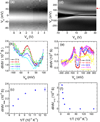
ApoMb results. (a) Differential conductance (dI/dV) measured at T = 77K as a function of bias and gate voltages. Gray scale from 1.56 × 10⁻⁵ S (black) to 2.64 × 10⁻⁵ S (white). (b) dI/dV measured at VG = 0 for various temperatures. (c) dI/dV of peak in (b) as a function of 1/T. (d) dI/dV for another Mb sample [gray scale from 0 (black) to 5.0 × 10⁻⁶ S (white)] measured at T = 6 K. The red arrow points to a possible vibration-assisted conduction line. (e) dI/dV at VG = 0 for various temperatures. (f) Conduction at VB = 0 and VG = 0 for sample in (d) as a function of 1/T.
Figure 5
Figure 5
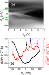
Mb results. (a) dI/dV as function of VB and VG at T = 6 K [gray scale is 0 (black) to 1.33 × 10⁻⁵ S (white)]. Green arrows point to conduction lines corresponding to Fe-His vibration-assisted tunneling. (b) dI/dV (black) and d2I/dV2 (red) spectra at VG = 11 V. Vertical arrows correspond to inelastic tunneling peaks.
Figure 6
Figure 6
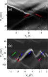
(a) Differential conductance (dI/dV) data from a Mb sample [gray scale from 0 (black) to 5.0 × 10⁻⁶ S (white)] at T = 6 K. The red arrows point to vibration-assisted conduction lines. (b) Differential conductance T = 6 K [gray scale from −0.27 × 10⁻⁶ S (black) to 1.6 × 10⁻⁶ S (white)] for another Mb sample. The blue arrows point to regions of negative differential conductance (NDC). The green arrow points to a faint conductance line independent of VG. The red arrow points to another conductance line possibly arising from a vibrational-assisted tunneling process or an excited electronic level in the protein(s).
Figure 7
Figure 7
Heme group structure (a) and energies of Fe d-orbitals in dry metMb (b).
Figure 8
Figure 8
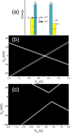
(a) Two-step electron transfer by redox center. δE is the difference in conformational energies between the unoccupied and occupied states. The Fermi levels of the source and drain electrodes are indicated by μS and μD, respectively. (b) Calculated differential conductance dI/dV as a function of bias and gate voltages VB and VG for T = 6 K, δE = 0 mV, VC = 0.307 V, CD : CS : CG = 24 : 40 : 1, tunneling rate 10 GHz (between the protein and the source or drain electrodes). CD, CS and CG are the capacitances of the drain, source, and gate electrical contacts, respectively. There is no two-step process in this case (δE = 0). (c) Calculated dI/dV with a two-step process for δE = 10 mV, other parameters same as in (b). See Appendix A for description of calculation.

References

    1. Munier B, de Visser SP, Shaik S. Chemical Reviews. 2004;104:3947–3980. pMID: 15352783 (Preprint http://pubs.acs.org/doi/pdf/10.1021/cr020443g) URL http://pubs.acs.org/doi/abs/10.1021/cr020443g. - DOI - DOI - PubMed
    1. Marcus RA, Sutin N. Biochimica et Biophysica Acta (BBA) - Reviews on Bioenergetics. 1985;811:265–322. ISSN 0304-4173 URL http://www.sciencedirect.com/science/article/pii/030441738590014X.
    1. Bendall DS. Protein Electron Transfer. Oxford: BIOS Publishers; 1996.
    1. Tao NJ. Phys. Rev. Lett. 1996;76(21):4066–4069. URL http://link.aps.org/doi/10.1103/PhysRevLett.76.4066. - DOI - PubMed
    1. Chi Q, Farver O, Ulstrup J. Proceedings of the National Academy of Sciences of the United States of America. 2005;102:16203–16208. (Preprint http://www.pnas.org/content/102/45/16203.full.pdf+html) URL http://www.pnas.org/content/102/45/16203.abstract. - PMC - PubMed

Publication types