. 2012 Sep 28;337(6102):1640-4.
doi: 10.1126/science.1226325.

A physically transient form of silicon electronics

Affiliations

A physically transient form of silicon electronics

Suk-Won Hwang et al. Science. .

Abstract

A remarkable feature of modern silicon electronics is its ability to remain physically invariant, almost indefinitely for practical purposes. Although this characteristic is a hallmark of applications of integrated circuits that exist today, there might be opportunities for systems that offer the opposite behavior, such as implantable devices that function for medically useful time frames but then completely disappear via resorption by the body. We report a set of materials, manufacturing schemes, device components, and theoretical design tools for a silicon-based complementary metal oxide semiconductor (CMOS) technology that has this type of transient behavior, together with integrated sensors, actuators, power supply systems, and wireless control strategies. An implantable transient device that acts as a programmable nonantibiotic bacteriocide provides a system-level example.


Figures

Figure 1
Figure 1. Demonstration platform for transient electronics, with key materials, device structures, and reaction mechanisms
a, Image of a transient electronic platform that includes all essential materials and several representative device components -- transistors, diodes, inductors, capacitors and resistors, with interconnects and interlayer dielectrics, all on a thin silk substrate. b, Exploded view schematic illustration of this device, with a top view in the lower right inset. All of the materials -- silicon nanomembranes (Si NMs; semiconductor) and thin films of magnesium (Mg, conductor), magnesium oxide (MgO, dielectric) silicon dioxide (SiO2, dielectric) and silk (substrate and packaging material) -- are transient, in the sense that they disappear by hydrolysis and/or simple dissolution in water. c, Images showing the time sequence of this type of physical transience, induced by complete immersion in water. d, Chemical reactions for each of the constituent materials with water.
Figure 2
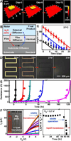
Figure 2. Experimental study of transient electronic materials and corresponding theoretical analysis
a, Atomic force microscope (AFM) topographical images of a single crystalline silicon nanomembrane (Si NM; initial dimensions: 3 µm × 3 µm × 70 nm), at various stages of dissolution by hydrolysis in phosphate buffered saline (PBS). b, Diagram of the processes of transport, adsorption, diffusion, reaction and desorption used in theoretical models of the transience. c, Experimental results (symbols) and simulations (lines) for the time dependent dissolution of Si NMs with different thicknesses, 35 nm (black), 70 nm (blue), 100 nm (red) in PBS at 37 °C. d, Optical microscope images of the dissolution of a serpentine trace of Mg (150 nm thick) trace on top of a layer of MgO (10 nm thick). e, Experimental (symbols) and simulation (lines) results showing the ability to tune the dissolution time of similar traces of Mg (300 nm thick) by use of different encapsulation layers of different materials. Here, measurements of length-normalized resistance show that the transience times increase progressively with encapsulation layers of MgO (400 nm, red; 800 nm, blue) and silk (condition i, cyan; condition ii, purple). With these simple schemes, the transience times can be adjusted in a range from minutes to several days. Silk packaging strategies can further extend these times.
Figure 3
Figure 3. Images and electrical prroperties of transient electronic components, circuits and sensors, including simple integrated circuits and sensor arrays
a, Image of LC (inductor-capacitor) oscillator fabricated with Mg electrodes and MgO dielectric layers (left) and silicon diodes with serpentine Mg resistors (right). b, Measurements of the S21 scattering parameter of an inductor (blue), capacitor (black), and LC oscillator (red) at frequencies up to 3 GHz. c, Images of an array of p-channel (left) metal-oxide semiconductor field effect transistors (MOSFETs) and a logic gate (inverter; right) comprised of n-channel MOSFETs. Each MOSFET consists of Mg source, drain, gate electrodes, MgO gate dielectrics and Si NM semiconductors. The inverter uses Mg for interconnects, and Au for source, drain, gate electrodes, in a circuit configuration shown in the diagram. d, Current-voltage (I-V) characteristics of a representative n-channel MOSFET (left, channel length (L) and width (W) are 20 µm and 900 µm, respectively). The threshold voltage, mobility and on/off ratio are −0.2 V, 660 cm2/V·s, and > 105, respectively. Transfer characteristic for the inverter (right, L and W are 20 µm and 700 µm for input transistor and 500 µm and 40 µm for load transistor, respectively). The voltage gain is ~8. e, Image of a collection of strain sensors based on Si NM resistors (left) and matrix of Si NM photodetectors with blocking diodes. In both cases, Mg serves as contact and interconnection electrodes and MgO as dielectric layers. f, Fractional change in resistance of a representative strain gauge as a function of time during cyclic loading (left). Bending induces tensile (red) and compressive (blue) strains, uniaxially up to ~0.2 %. Image collected with the photodetector array (right). Inset shows the original image taken by the photodetector array. g, Images of logic gates in which controlled transience affects functional transformation, in this case from NOR (left) to NAND (right) operation, by selective dissolution of an unencapsulated Mg interconnect. h, Output voltage characteristics of the circuits before (NOR, left) and after (NAND, right) transformation. Va and Vb represent voltage inputs.
Figure 4
Figure 4. In vivo evaluations and example of a transient bio-resorbable device for thermal therapy
a, Image of implantation of a demonstration platform for transient electronics in the dorsal region of a BALB-c mouse (left). Implant site after 3 weeks (right). b, Histological section of tissue at the implant site, excised after 3 weeks, showing the remainder of the silk film. (A, subcutaneous tissue; B, silk film; C, muscle layer). c, Transient wireless device for thermal therapy, consisting of two resistors (red outline) connected to a first wireless coil (70 MHz; outer coil) and a second resistor (blue outline) connected to a second, independently addressable, wireless coil (140 MHz; inner coil). d, Thermal image of this device coupled with a primary coil driven on resonance with the outer coil. Here, the two outer resistors (Re) are powered, to generate local heating (left). The thermal image on the right shows the case where the primary is operated at two frequencies, to drive both the inner and outer coils simultaneously. e, Primary coil next to a sutured implant site for a transient thermal therapy device (left). Inset shows the image of a device. Thermal image collected while wirelessly powering the device through the skin; the results show a hot spot (5 °C above background) at the expected location (right), with magnified view in the inset.

Comment in

References

    1. Bettinger CJ, Bao Z. Organic Thin-Film Transistors Fabricated on Resorbable, Biomaterial Substrates. Adv. Mater. 2010;22:651–655. - PMC - PubMed
    1. Irimia-Vladu M, et al. Biocompatible and Biodegradable Materials for Organic Field-Effect Transistors. Adv. Funct. Mater. 2010;20:4069–4076.
    1. Legnani C, et al. Bacterial cellulose membrane as flexible substrate for organic light emitting devices. Thin Solid Films. 2008;517:1016–1020.
    1. Kim D-H, et al. Dissolvable Films of Silk Fibroin for Ultrathin, Conformal Bio-Integrated Electronics. Nature Mater. 2010;9:511–517. - PMC - PubMed
    1. Wang Y, et al. In vivo degradation of three-dimensional silk fibroin scaffolds. Biomaterials. 2008;29:3415–3428. - PMC - PubMed

Publication types