. 2013 Mar;12(3):246-52.
doi: 10.1038/nmat3518. Epub 2012 Dec 16.

Vertically stacked multi-heterostructures of layered materials for logic transistors and complementary inverters

Affiliations

Vertically stacked multi-heterostructures of layered materials for logic transistors and complementary inverters

Woo Jong Yu et al. Nat Mater. 2013 Mar.

Abstract

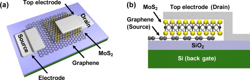
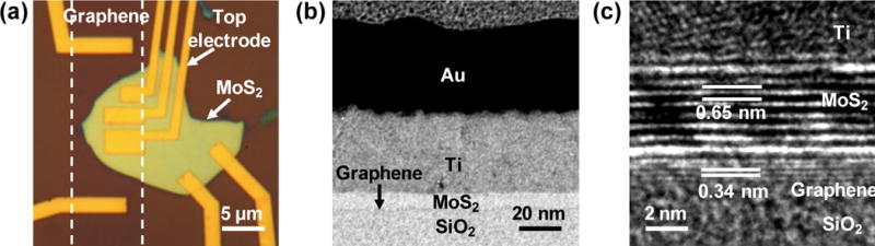
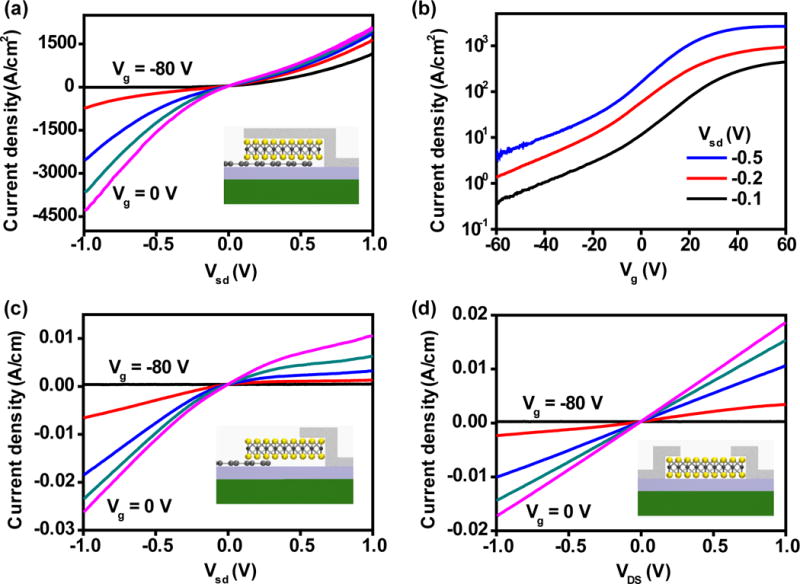
Graphene has attracted considerable interest for future electronics, but the absence of a bandgap limits its direct applicability in transistors and logic devices. Recently, other layered materials such as molybdenum disulphide (MoS(2)) have been investigated to address this challenge. Here, we report the vertical integration of multi-heterostructures of layered materials for the fabrication of a new generation of vertical field-effect transistors (VFETs) with a room temperature on-off ratio > 10(3) and a high current density of up to 5,000 A cm(-2). An n-channel VFET is created by sandwiching few-layer MoS(2) as the semiconducting channel between a monolayer graphene sheet and a metal thin film. This approach offers a general strategy for the vertical integration of p- and n-channel transistors for high-performance logic applications. As an example, we demonstrate a complementary inverter with a larger-than-unity voltage gain by vertically stacking graphene, Bi(2)Sr(2)Co(2)O(8) (p-channel), graphene, MoS(2) (n-channel) and a metal thin film in sequence. The ability to simultaneously achieve a high on-off ratio, a high current density and a logic function in such vertically stacked multi-heterostructures can open up possibilities for three-dimensional integration in future electronics.


Conflict of interest statement

Author Information. The authors declare no competing financial interests. Reprint and permissions information is available at www.nature.com/reprints.

Figures

Figure 1
Figure 1. Schematic illustration of the vertically stacked graphene-MoS2-metal field-effect transistors
a, A schematic illustration of the three-dimensional view of the device layout. b, A schematic illustration of the cross-sectional view of the device, with the graphene and top metal thin film functioning as the source and drain electrodes, the MoS2 layer as the vertically stacked semiconducting channel and its thickness defines the channel length. Silicon back gate is used with 300-nm SiO2 dielectric layer.
Figure 2
Figure 2. Fabrication and structural characterization of the vertical transistor
a, An optical image of a typical vertical transistor device. Bottom graphene electrode is shaped to stripes of 10 μm width. Multi-layer MoS2 is located on the graphene electrode and top metal electrode is located on MoS2 to overlap with bottom graphene electrode to enable vertical current flow. b, A cross-sectional TEM image of a vertical transistor. c, A cross-sectional HRTEM image of the interface between multi-layer graphene, multi-layer MoS2 and top electrode of Ti. A TEM image of multilayer graphene device is shown here for better illustration because it is difficult to visualize the monolayer graphene electrode due to significant electron-beam damage while conducting the TEM studies.
Figure 3
Figure 3. Room temperature electrical properties of the vertical and planar transistors
a, Isd-Vsd output characteristics of a vertical transistor. The current is normalized by the area. b, Isd-Vgs transfer characteristics of the device shown in a at Vsd = −0.1, −0.2, and −0.5 V. c, Isd-Vsd output characteristics of a planar transistor with MoS2 channel between a graphene electrode and metal electrode. d, Ids-Vsd output characteristics of a planar transistor with two top metal electrodes on planar MoS2 channel. The current is normalized by the width of the electrode in c and d. The back-gate voltage is varied from −80 V to 0 V in the step of 20 V in a, c and d. Insets in a, c and d shows the schematics of the transistor structure for each output characteristics.
Figure 4
Figure 4. Schematic illustration of the band diagrams of the vertical transistors and the electrical characteristics
a, The schematic illustration of a vertical transistor. Gate electric field is applied from silicon back gate located bottom of graphene and grounded top electrode. b, c, The band structure at negative source bias at graphene (b, Vsd<0) and positive source bias at graphene (c, Vsd>0) under positive (solid) or negative (dashed) Vg. d, Transfer characteristics of a VFET at different temperature from 290 K to 150 K. The inset shows the corresponding on-off ratio variation. e, Temperature dependent diode characteristics. Each curve from bottom to top is obtained at different Vg from −60 V to 60 V with 20 V step variation. The inset shows corresponding Schottky barrier height variation obtained from the slope of the fitted line. f, The simulated on-current density of graphene-MoS2-graphene tunneling barrier (GMG TB, blue line), graphene-MoS2-Metal(Ti) Schottky barrier (GMM SB, black line), and graphene-MoS2-graphene Schottky barrier (GMG SB, red line) at bias of −0.1 V. Experimental on-current density are plotted by black square (■) for GMM SB and red circle ( formula image
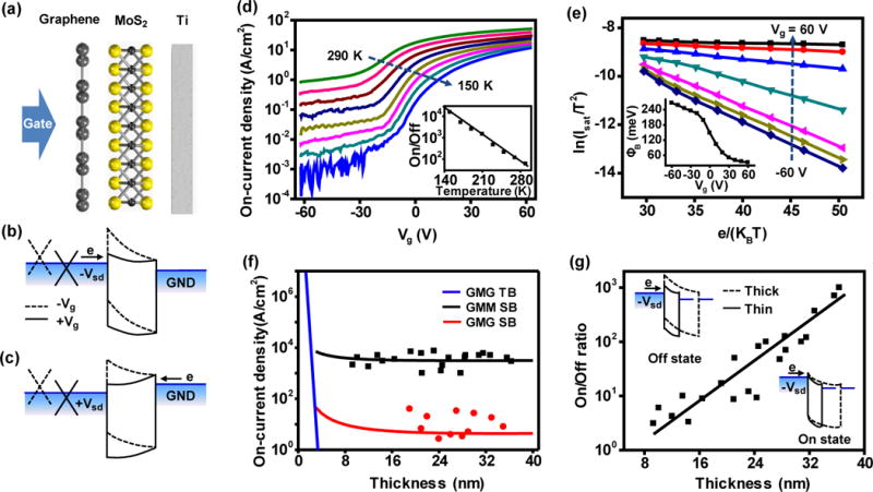
) for GMG SB at Vsd = −0.5 V. g, The on-off current ratio of the vertical transistors with various channel length (thickness of MoS2). The on- and off-state band diagrams for thin (solid) and thick (dashed) MoS2 layers are represented in the insets.
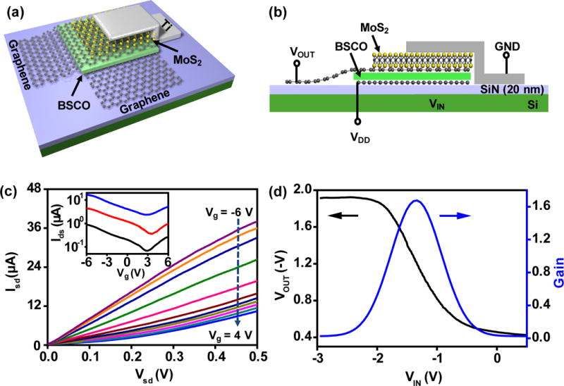
Figure 5
Figure 5. Vertically stacked multi-heterostructures of layered materials for complementary inverters
a, Three dimensional schematic illustration of a complementary inverter by vertically stacking the layered materials of graphene, Bi2Sr2Co2O8 (BSCO) (p-channel), graphene, MoS2 (n-channel), and metal thin film on Si/SiNx (20 nm) substrate. b, Cross-sectional view of the vertically stacked inverter. c, Output characteristics of a p-channel Bi2Sr2Co2O8 VFET with top and bottom graphene electrodes on Si/SiNx (20 nm) substrate. The back-gate voltage is varied from −6 V (top) to 4 V (bottom) in the step of 1 V. The inset shows the transfer characteristics of Bi2Sr2Co2O8 VFET at Vsd = −0.2, −0.05, and −0.01 V from top to bottom. d, The inverter characteristics from vertically stacked p- and n-type VFETs. A negative supply voltage (VDD=−2V) is applied to bottom graphene, and the gain of the inverter is ~1.7.

References

    1. Novoselov KS, et al. Electric field effect in atomically thin carbon films. Science. 2004;306:666–669. - PubMed
    1. Novoselov KS, et al. Two-dimensional gas of massless Dirac fermions in graphene. Nature. 2005;438:197–200. - PubMed
    1. Dean CR, et al. Boron nitride substrates for high-quality graphene electronics. Nat Nanotechnol. 2010;5:722–726. - PubMed
    1. Wu YQ, et al. High-frequency, scaled graphene transistors on diamond-like carbon. Nature. 2011;472:74–78. - PubMed
    1. Liao L, et al. High-speed graphene transistors with a self-aligned nanowire gate. Nature. 2010;467:305–308. - PMC - PubMed

Publication types