. 2013 Jan 2;110(1):40-5.
doi: 10.1073/pnas.1210417110. Epub 2012 Dec 17.

Conformal surface plasmons propagating on ultrathin and flexible films

Affiliations

Conformal surface plasmons propagating on ultrathin and flexible films

Xiaopeng Shen et al. Proc Natl Acad Sci U S A. .

Abstract

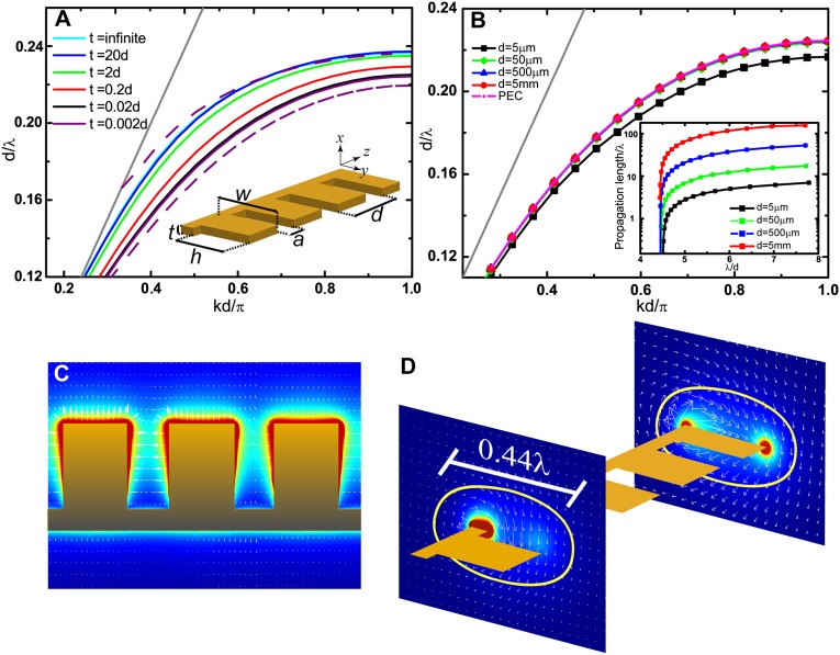
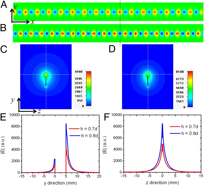
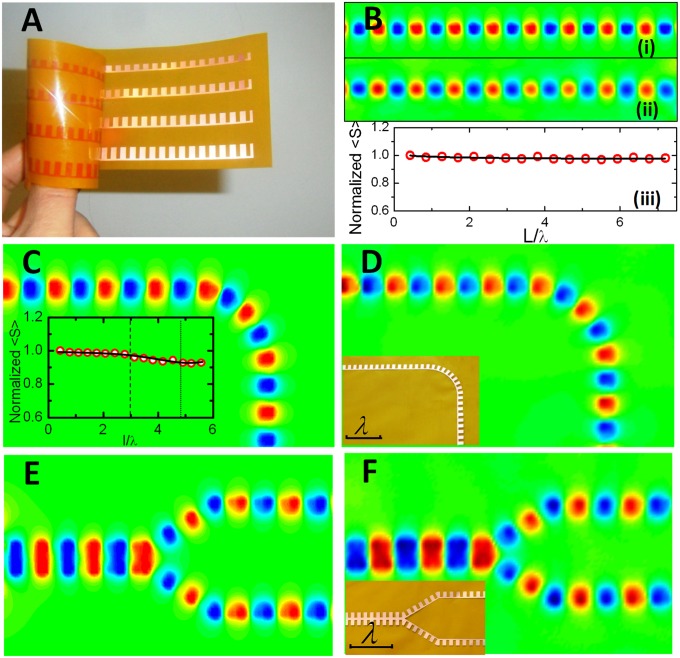
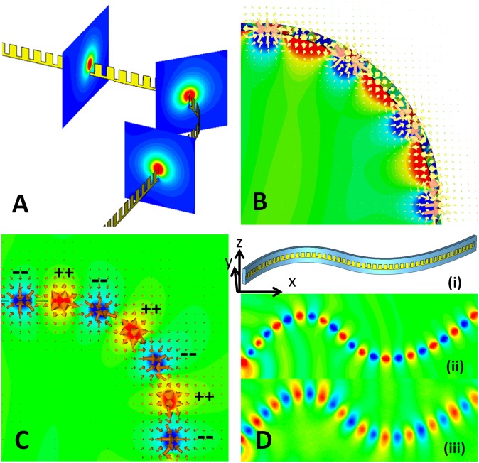
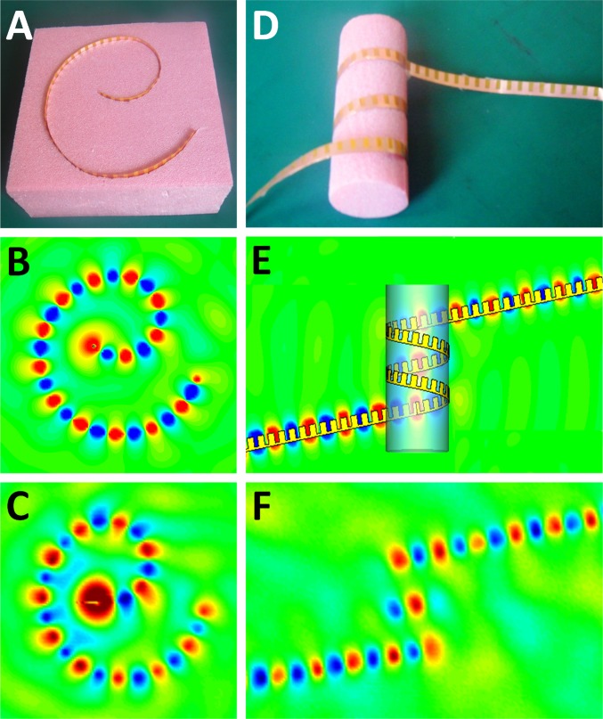
Surface plasmon polaritons (SPPs) are localized surface electromagnetic waves that propagate along the interface between a metal and a dielectric. Owing to their inherent subwavelength confinement, SPPs have a strong potential to become building blocks of a type of photonic circuitry built up on 2D metal surfaces; however, SPPs are difficult to control on curved surfaces conformably and flexibly to produce advanced functional devices. Here we propose the concept of conformal surface plasmons (CSPs), surface plasmon waves that can propagate on ultrathin and flexible films to long distances in a wide broadband range from microwave to mid-infrared frequencies. We present the experimental realization of these CSPs in the microwave regime on paper-like dielectric films with a thickness 600-fold smaller than the operating wavelength. The flexible paper-like films can be bent, folded, and even twisted to mold the flow of CSPs.


Conflict of interest statement

The authors declare no conflict of interest.

Figures

Fig. 1.
Fig. 1.
Dispersion relationships and local field distributions of the comb-shaped CSP structures. (A) Normalized dispersion relations for the fundamental CSP mode as a function of thickness, t. (Inset) Geometric parameters of the structure, with W = d, a = 0.4d, and h = 0.8d fixed for all curves. The metal is modeled as a PEC. Continuous lines render the dispersion relations of single comb-shaped structures for different values of t, whereas the two dashed lines correspond to a double comb-shaped structure with t = 0.02d. (B) Variation of the dispersion relation with different values of d using copper optical constants and the same geometric parameters as in A for t = 0.02d. The PEC curve from A is also displayed for comparison purposes. (Inset) Propagation lengths normalized to the operating wavelength for the same values of d as in the main panel. (C) Amplitude (modulus) of the electric field evaluated at the yz plane that cuts the metal symmetrically, with the color scale ranging from red (highest amplitude) to dark blue (lowest amplitude). The white arrows depict the yz components of the electric field, showing its phase variation along the propagation direction. (D) Power flow contour plots evaluated at two transverse xy planes cutting the grooves (Left) and teeth (Right) of the comb-shaped structure. The color scale ranges from red (highest intensity) to dark blue (lowest intensity), and the white arrows depict the xy components of the magnetic field. The orange line denotes the modal size of the CSP mode, which represents 70% of the integrated energy flow. All geometric parameters in C and D correspond to those in B, with d = 5 mm and an operating wavelength of 30 mm.
Fig. 2.
Fig. 2.
Propagation of surface EM waves and field confinements on two ultrathin corrugated metal strips (W = d, t = 0.0036d, a = 0.4d, and d = 5 mm) with different groove depths (h = 0.8d and h = 0.7d). The operating frequency is 12 GHz (λ = 25 mm). An electric monopole pointing to the y direction with unit current is used for excitation at the left edge. (A and B) Simulated amplitudes of electric fields (|E|) on the two corrugated metal strips (A: h = 0.8d; B: h = 0.7d) over a length of 400 mm (16λ). (C and D) Field distributions on the cross-sections of the two corrugated metal strips (C: h = 0.8d; D: h = 0.7d) located 300 mm (12λ) away from the source (the dashed line in A and B). The black lines indicate the cross-sections of the two strips. The CSP modes are tightly confined to the corrugated strips with strong field enhancements. (E and F) Electric field distributions along the vertical cut (E) and horizontal cut (F), shown by the orthogonal dashed lines in C and D. The fields near the deeply corrugated strip (h = 0.8d) are much stronger and decay exponentially faster compared with those of the shallowly corrugated strip (h = 0.7d) along the two orthogonal directions.
Fig. 3.
Fig. 3.
Simulation and measurement results of CSP waves on planar surfaces at 10 GHz. (A) Photograph of the nearly zero-thickness CSP structures on a flexible and ultrathin dielectric film, which can be wrapped on arbitrarily curved surfaces. The four CSP strips shown have groove depths h, from top to bottom, of 3, 4, 5, and 6 mm. Here a = 2 mm, d = 5 mm, t = 0.018 mm, and W = h + 1 mm. (B) Simulation (i) and measurement (ii) results of electric field (Ez) distributions along the ultrathin corrugated metal strip with groove depth h = 3 mm. (iii) Normalized time-averaged power densities (peak values) along an observation line (l) lying 1.5 mm above the corrugated edge. (C and D) Simulated (C) and measured (D) electric fields (Ez) of the 90o bend. (C, Inset) Normalized time-averaged power densities (peak values) along a bending observation line (l) lying 1.5 mm above the corrugated edge, in which the region between two thin dashed lines is the bending path. (D, Inset) Photograph of an experimental sample, with a = 2 mm, d = 5 mm, h = 4 mm, W = 5 mm, and t = 0.018 mm. (E and F) Simulated (E) and measured (F) electric fields (Ez) of the 60o Y-splitter. (F, Inset) Photograph of an experimental sample, with a = 2 mm, d = 5 mm, h = 4 mm, W = 5 mm, and t = 0.018 mm. In all cases, an electric monopole parallel to the plane was used to excite the CSP modes at the left edge.
Fig. 4.
Fig. 4.
Simulation and measurement results of CSP waves on curved surfaces at 10 GHz. (A) An ultrathin corrugated metal strip (W = d, t = 0.0036d, h = 0.8d, a = 0.4d, and d = 5 mm) that is bent vertically by 90° with a bending radius of 30 mm, and numerical simulation results of power-density distributions on three different cross-sections before bending, at the bending center, and after bending. (B) 3D distribution of CSP modes across the bend, in which the arrows represent the vector E-fields and color scales indicate the field amplitudes. (C) Top view of the vector E-field distribution across the bend, clearly showing the generation of surface charges. (D) Simulation and experimental results of electric field distributions (Ez) on a vertically S-bending surface. (i) CSP structure on the S-bending surface. (ii) Simulation result. (iii) Experimental result. CSP waves creep through the bending surface smoothly. In both cases, an electric monopole pointing to the z direction is used for excitation at the left edge.
Fig. 5.
Fig. 5.
Simulation and measurement results of CSP waves on a spiral surface and a 3D helical-shaped curved surface. (A) Fabricated sample of the spiral-shaped ultrathin CSP film with an initial curvature radius of 20 mm and a maximum curvature radius of 40 mm, in which a = 2 mm, d = 5 mm, h = 4 mm, w = 5 mm, and t = 0.018 mm. The CSP film is supported by a foam substrate with nearly unity dielectric constant. (B and C) Full-wave simulation (B) and experimental (C) results of electric field distributions (Ey) at 11 GHz on the plane lying 1.5 mm above the spiral sample. An electric monopole perpendicular to the foam surface (Fig. S2B) was used to excite the CSP modes at the inner edge. (D) Fabricated sample of the ultrathin CSP film that is wrapped on a foam cylinder spirally at a bevel angle of 10°. The foam cylinder had a radius of 15 mm and was buried in the foam background to allow measurement of the fringe and pillar regions of the CSP strip. An electric monopole parallel to the corrugated film was used to excite the CSP modes at the left edge. (E) Full-wave simulation results of electric field distributions (Ez) along the 3D helix path at 11 GHz. (F) Experimental results of electric field distributions at 11 GHz on the plane lying 1.5 mm above the top of the foam cylinder. Excellent performance of the CSP propagation is observed along the helical-shaped surface in both the simulation and the measurement results.

Similar articles

Cited by

References

    1. Ritchie RH. Plasma losses by fast electrons in thin films. Phys Rev. 1957;106:874–881.
    1. Barnes WL, Dereux A, Ebbesen TW. Surface plasmon subwavelength optics. Nature. 2003;424(6950):824–830. - PubMed
    1. Maier SA. Plasmonics: Fundamentals and Applications. New York: Springer; 2007.
    1. Tsai W-H, Tsao Y-C, Lin H-Y, Sheu B-C. Cross-point analysis for a multimode fiber sensor based on surface plasmon resonance. Opt Lett. 2005;30(17):2209–2211. - PubMed
    1. Fang N, Lee H, Sun C, Zhang X. Sub-diffraction-limited optical imaging with a silver superlens. Science. 2005;308(5721):534–537. - PubMed

Publication types

MeSH terms

LinkOut - more resources