. 2013 Jan 22;7(1):834-43.
doi: 10.1021/nn305400n. Epub 2012 Dec 28.

Electrochemistry at the edge of a single graphene layer in a nanopore

Affiliations

Electrochemistry at the edge of a single graphene layer in a nanopore

Shouvik Banerjee et al. ACS Nano. .

Abstract

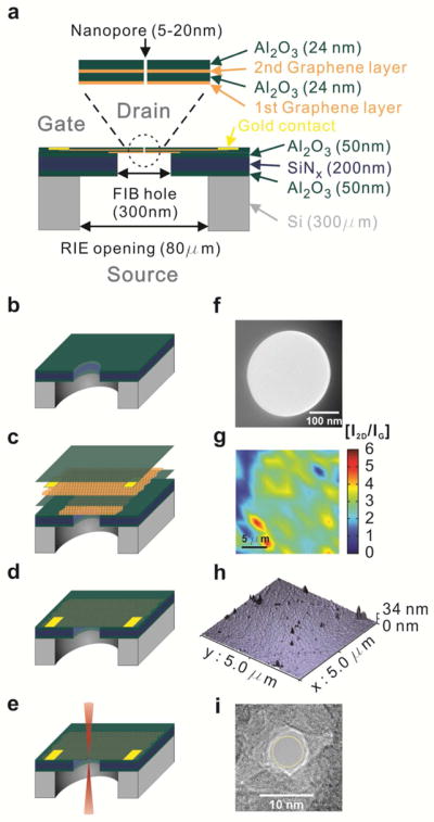
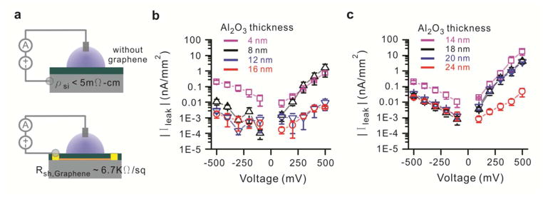
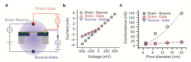
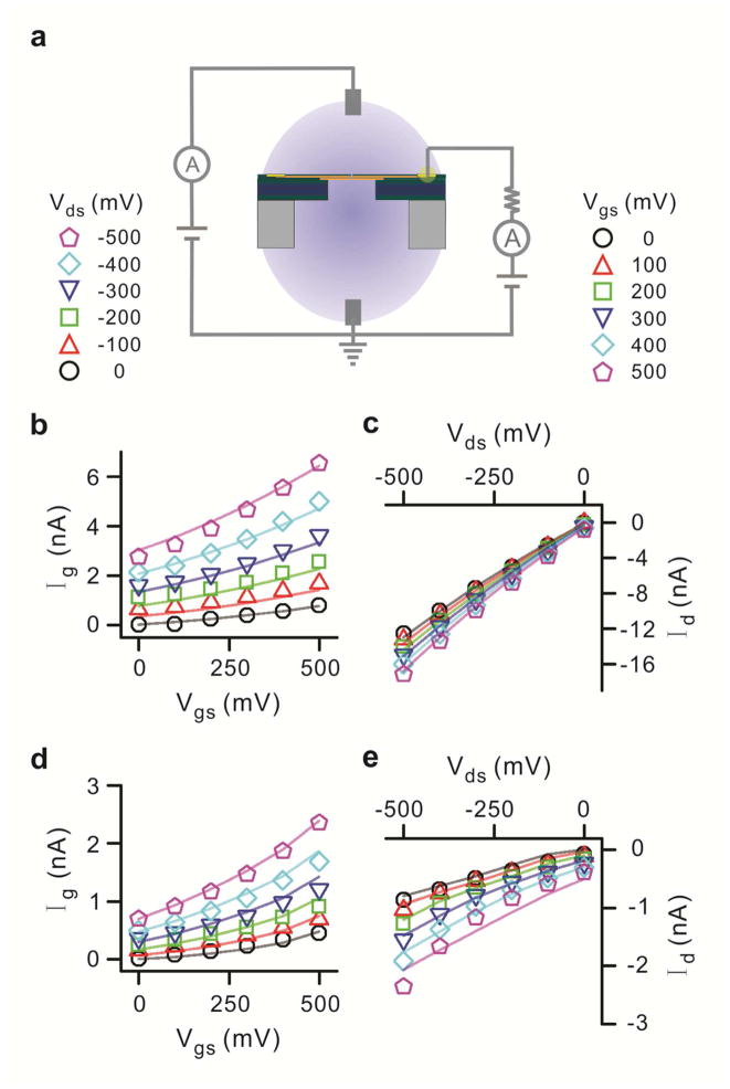
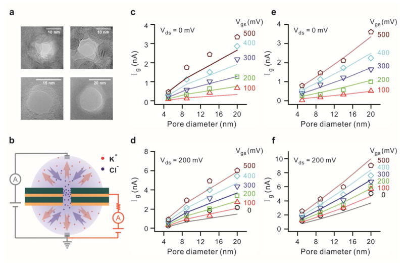
We study the electrochemistry of single layer graphene edges using a nanopore-based structure consisting of stacked graphene and Al(2)O(3) dielectric layers. Nanopores, with diameters ranging from 5 to 20 nm, are formed by an electron beam sculpting process on the stacked layers. This leads to a unique edge structure which, along with the atomically thin nature of the embedded graphene electrode, demonstrates electrochemical current densities as high as 1.2 × 10(4) A/cm(2). The graphene edge embedded structure offers a unique capability to study the electrochemical exchange at an individual graphene edge, isolated from the basal plane electrochemical activity. We also report ionic current modulation in the nanopore by biasing the embedded graphene terminal with respect to the electrodes in the fluid. The high electrochemical specific current density for a graphene nanopore-based device can have many applications in sensitive chemical and biological sensing, and energy storage devices.


Figures

Figure 1
Figure 1
Schematic diagram of graphene-embedded stacked membrane structure and fabrication. (a) Schematic showing the thickness of each layer as well as diameters of RIE, FIB and nanopore holes (b) Supporting membrane consists of three layers of 50 nm of Al2O3, 200 nm of SiNx and 50 nm of Al2O3, deposited on 300 μm-thick double polished prime Si wafer. RIE is used to etch 80 μm-wide opening in Si wafer to supporting membrane and 300 nm through hole is fabricated in supporting membrane by FIB. (c) First graphene layer transferred onto the FIB hole acts as the support for subsequent layers. This is insulated from the second graphene layer by 24 nm of Al2O3 deposition. Second graphene layer, which is the active electrode at the middle of membrane, is transferred onto first Al2O3 layer. Ti/Au deposition enables the formation of contacts. A further layer of Al2O3 is deposited to insulate the electrode from the ionic solution. (d) Final structure of graphene embedded membrane suspended on 300 nm FIB hole. (e) Focused electron beam (CBED mode) in TEM is used to fabricate a single nanopore of 5 to 20 nm diameter. (f) TEM image of FIB hole of 300 nm diameter in supporting membrane. (g) Raman spectroscopy of I2D/IG obtained from graphene surface indicating predominantly monolayer coverage. (h) AFM image of membrane surface. Roughness (Ra = 1.89 ± 0.67 nm) is significantly reduced on deposition of Al2O3 on graphene compared to bare graphene surface (Ra = 0.84 ± 0.21 nm). (i) 5nm nanopore is fabricated by convergent electron beam in TEM.
Figure 2
Figure 2
Leakage test on various thickness of Al2O3. (a-top) Schematics showing leakage measurement setup for Al2O3 on p++ Silicon (ρ < 5 mΩ-cm). Al2O3 of thickness 4 to 16 nm were deposited on the conductive Si wafer. Measurements are conducted with one electrode connected to Si wafer and the other attached to Ag/AgCl electrode in the solution (a-bottom) Schematic of leakage measurement setup for Al2O3 on graphene transferred onto Si surface with Al2O3 deposited on top. Al2O3 thickness in range of 14 to 24 nm is deposited on graphene (Rsh ≈ 6.7 kΩ/sq) transferred on Si wafer with a ALD deposited Al2O3 top surface. Measurements are conducted between the graphene film contacted with aluminium wires and the solution contacted with Ag/AgCl electrodes. All leakage experiments are performed in 1 M KCl, 10 mM Tris, 1 mM EDTA at pH 7.6 and at room temperature (22 ± 2 °C). (b) Leakage current density measured for Al2O3 on conductive Silicon. Al2O3 thickness less than 10 nm showed leakage current greater than 1 nA/mm2 at 500 mV, but thicker Al2O3 (>10 nm) showed much greater insulation over the voltage range of −500 mV to +500 mV. (c) Leakage current density for Al2O3 deposited on graphene. Leakage current is observed to be fairly high up to 20 nm-thick Al2O3. Also the leakage is significantly higher for positive voltage at Ag/AgCl electrode. 24 nm-thick Al2O3 displays decent insulation from leakage. Current leakage occurrence at relative thicker Al2O3 deposited on graphene is associated with wrinkles on graphene (Supplementary Fig. 9).
Figure 3
Figure 3
Electrochemical measurements for embedded graphene nanoelectrode. (a) Schematic diagram of measurement setup. For the drain-source measurement (gray), source is connected to ground and voltage applied at the drain. For drain-gate (red) and drain-source (blue) measurements, the gate is connected to ground and voltage is applied to the other terminal. (b) Current-voltage curve of nanopore ionic current and electrochemical behavior of graphene edge through 5 nm nanopore. Identical currents through the drain-gate and source-gate pathways indicate electrochemical exchange at the exposed graphene edge. (c) Conductance dependence on pore diameter. Drain-source conductance shows a square dependence on pore diameter, while gate current exchange shows a fairly linear dependence on pore diameter consistent with electrochemical exchange at cylindrical nanopore wall. The slight variation from linear dependence is may be attributed to varying graphene sheet thickness on various regions of the membrane. 5, 9, 14 and 20 nm diameter nanopores were used in this study. All experiments are performed in 1 M KCl, 10 mM Tris, 1 mM EDTA at pH 7.6
Figure 4
Figure 4
Three terminal measurement for the graphene embedded membrane. (a) Schematic diagram with source connected to ground while voltage is swept at the drain and gate terminals. (b) and (d) Gate current characteristics for 1 M KCl and 10 mM KCl respectively. The variation of gate current with gate source bias as drain voltage is varied is shown. The scatter points are experimental numbers while the straight lines are simulation fits. (c) and (e) Drain current characteristics for 1 M KCl and 10 mM KCl solution respectively. The variation of drain current with drain source bias as gate voltage is varied is recorded. Both solutions are prepared with 10 mM Tris and 1 mM EDTA for buffering at pH 7.6.
Figure 5
Figure 5
Gate current dependence on pore diameter (a) TEM images of nanopores of four different diameters (5, 9, 14, 20 nm) nanopores drilled through an embedded graphene membrane. (b) Schematic diagram of electrochemistry. The positive gate bias leads to attraction of chloride ions to the nanopore and expulsion of potassium ions. Red dots and arrows represent potassium ions while blue dots and arrows are for chloride ions. (c–f) Scaling of gate current with pore size at drain bias of 0 and −200 mV for 4 different pore diameters. (c), (d) Gate current dependence on pore diameter using 10 mM KCl solution. Linear dependence on pore diameter is observed over gate bias ranging from 0 to +500 mV for both drain bias values. (e), (f) Gate current dependence on pore diameter using 1 M KCl solution. Similar linear dependence on pore diameter is observed entire voltage range. The scatter points are experimental numbers while the straight lines are simulation fits. Both solutions are prepared with 10 mM Tris and 1 mM EDTA for buffering at pH 7.6

References

    1. Novoselov KS, Geim AK, Morozov SV, Jiang D, Zhang Y, Dubonos SV, Grigorieva IV, Firsov AA. Electric Field Effect in Atomically Thin Carbon Films. Science. 2004;10 :306, 666–669. - PubMed
    1. Bolotin KI, Sikes KJ, Jiang Z, Klima M, Fudenberg G, Hone J, Kim P, Stormer HL. Ultrahigh Electron Mobility in Suspended Graphene. Solid State Commun. 2008;146:351–355.
    1. Balandin AA. Thermal Properties of Graphene and Nanostructured Carbon Materials. Nat Mater. 2011;10:569–581. - PubMed
    1. Mak KF, Shan J, Heinz TF. Electronic Structure of Few-Layer Graphene: Experimental Demonstration of Strong Dependence on Stacking Sequence. Phys Rev Lett. 2010;104:176404. - PubMed
    1. Pumera M. Electrochemistry of Graphene: New Horizons for Sensing and Energy Storage. Chem Rec. 2009;9:211–223. - PubMed

Publication types