. 2013 Feb 13;13(2):746-51.
doi: 10.1021/nl304435z. Epub 2013 Jan 7.

Design and synthesis of diverse functional kinked nanowire structures for nanoelectronic bioprobes

Affiliations

Design and synthesis of diverse functional kinked nanowire structures for nanoelectronic bioprobes

Lin Xu et al. Nano Lett. .

Abstract

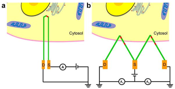
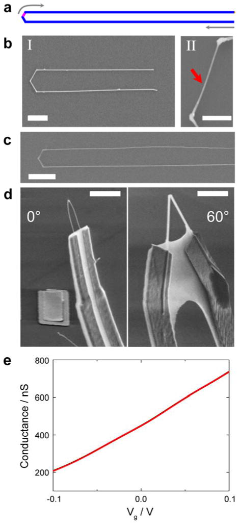
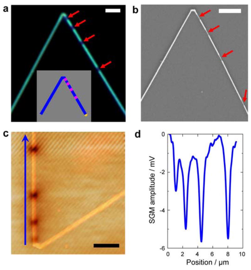
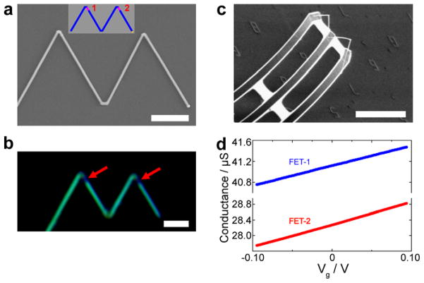
Functional kinked nanowires (KNWs) represent a new class of nanowire building blocks, in which functional devices, for example, nanoscale field-effect transistors (nanoFETs), are encoded in geometrically controlled nanowire superstructures during synthesis. The bottom-up control of both structure and function of KNWs enables construction of spatially isolated point-like nanoelectronic probes that are especially useful for monitoring biological systems where finely tuned feature size and structure are highly desired. Here we present three new types of functional KNWs including (1) the zero-degree KNW structures with two parallel heavily doped arms of U-shaped structures with a nanoFET at the tip of the "U", (2) series multiplexed functional KNW integrating multi-nanoFETs along the arm and at the tips of V-shaped structures, and (3) parallel multiplexed KNWs integrating nanoFETs at the two tips of W-shaped structures. First, U-shaped KNWs were synthesized with separations as small as 650 nm between the parallel arms and used to fabricate three-dimensional nanoFET probes at least 3 times smaller than previous V-shaped designs. In addition, multiple nanoFETs were encoded during synthesis in one of the arms/tip of V-shaped and distinct arms/tips of W-shaped KNWs. These new multiplexed KNW structures were structurally verified by optical and electron microscopy of dopant-selective etched samples and electrically characterized using scanning gate microscopy and transport measurements. The facile design and bottom-up synthesis of these diverse functional KNWs provides a growing toolbox of building blocks for fabricating highly compact and multiplexed three-dimensional nanoprobes for applications in life sciences, including intracellular and deep tissue/cell recordings.


Figures

Figure 1
Figure 1. Overview of KNW synthetic designs and potential applications
a, U-shaped KNW with integrated nanoFET (red) shown as a bioprobe for intracellular recording. b, W-shaped KNW with multiple nanoFETs (red) illustrated as a bioprobe for simultaneous intracellular/extracellular recording. In a and b, green indicates heavily-doped (n++) S/D NW nanoelectrode arms, red highlights the pointlike active nanoFET elements, and gold indicates the fabricated metal interconnects to the NW S/D arms. A schematic of a cell to scale is drawn with the different device designs to show the potential for achieving minimally invasive deep penetration (a) and multiplexed intracellular and extracellular recording (b).
Figure 2
Figure 2. U-shaped KNWs
a, Schematic of a U-shaped KNW with tip constructed from three 120° cis-linked kinks. The lightly-doped n-type nanoFET element (pink) is encoded at the tip and connected by heavily-doped n++ S/D arms (blue). The grey arrows indicate the growth sequence for the nanostructure. (b) SEM images of original (I: scale bare, 2 μm) and KOH-etched (II: scale bar, 500 nm) U-shaped KNW synthesized with 80 nm diameter Au-NP catalysts. Red arrow marks the position of nanoFET element between the second and the third cis-linked kinks. c, Representative SEM image of a U-shaped KNW prepared using 30 nm diameter Au-NPs. The measured nanowire diameter is 30 nm. Scale bar, 1 μm.. d, SEM images of 3D probe devices fabricated using a 30 nm diameter U-shaped (left) and 150 nm diameter V-shaped (right) KNW building blocks. Scale bars, 3 μm. e, Conductance versus water-gate reference potential data recorded from a representative 30 nm diameter U-shaped KNW 3D probe in 1× phosphate buffer saline (PBS).
Figure 3
Figure 3. Series nanoFET in V-shaped KNWs
a, Dark-field optical microscopy image of a KOH-etched KNW with 4 nanoFETs. The dark segments correspond to the four lightly doped nanoFET elements (red arrows). Scale bar, 2 μm. Inset, schematic of the synthetic design for the KNW with 4 series nanoFETs (pink) and heavily-doped connecting NW segments (blue). b, SEM image of the same KOH-etched KNW. Red arrows mark the positions of the preferentially-etched lightly-doped nanoFET channels. Scale bar, 2 μm. c, Superposition of scanning gate microscopy (SGM) and AFM topographic images for an unetched series KNW device, where the V-shaped KNW was synthesized in the same way as that shown in a and b; the tip voltage, Vtip, for the SGM image was −10 V. Scale bar, 2 μm. Dark regions in SGM image correspond to reduced NW conductance. d, Line profile of the SGM signal along the NW arm indicated by the blue arrow in c. The negative peaks correspond to the dark regions in SGM image.
Figure 4
Figure 4. Parallel nanoFET KNWs
a, SEM image of a W-shaped parallel-nanoFET KNW. Scale bar, 2 μm. Inset: Schematic of the W-shaped KNW with one nanoFET encoded at the tip of each V-shaped component of the “W”, where blue and pink indicate heavily-doped connections and lightly-doped nanoFET channels, respectively. b, Dark-field optical microscopy image of KOH etched W-shaped KNW. The two dark color segments correspond to the lightly doped nanoFET elements (red arrows) near the two tips. Scale bar, 2 μm. c, SEM image of W-shaped parallel-nanoFET KNW bend-up probe. Scale bar, 20 μm. d, Conductance versus water-gate reference potential data recorded independently from two parallel nanoFETs.

References

    1. Lieber CM. MRS Bull. 2011;36:1052–1063. - PMC - PubMed
    1. Tian B, Lieber CM. Pure Appl Chem. 2011;83:2153–2169. - PMC - PubMed
    1. Schmidt V, Wittemann JV, Gosele U. Chem Rev. 2010;110:361–388. - PubMed
    1. Mai L, Yang F, Zhao Y, Xu X, Xu L, Hu B, Luo Y, Liu H. Mater Today. 2011;14:346–353.
    1. Wang ZL. MRS Bull. 2012;37:814–827.

Publication types

LinkOut - more resources