. 2012:3:895-908.
doi: 10.3762/bjnano.3.100. Epub 2012 Dec 21.

Diamond nanophotonics

Affiliations

Diamond nanophotonics

Katja Beha et al. Beilstein J Nanotechnol. 2012.

Abstract

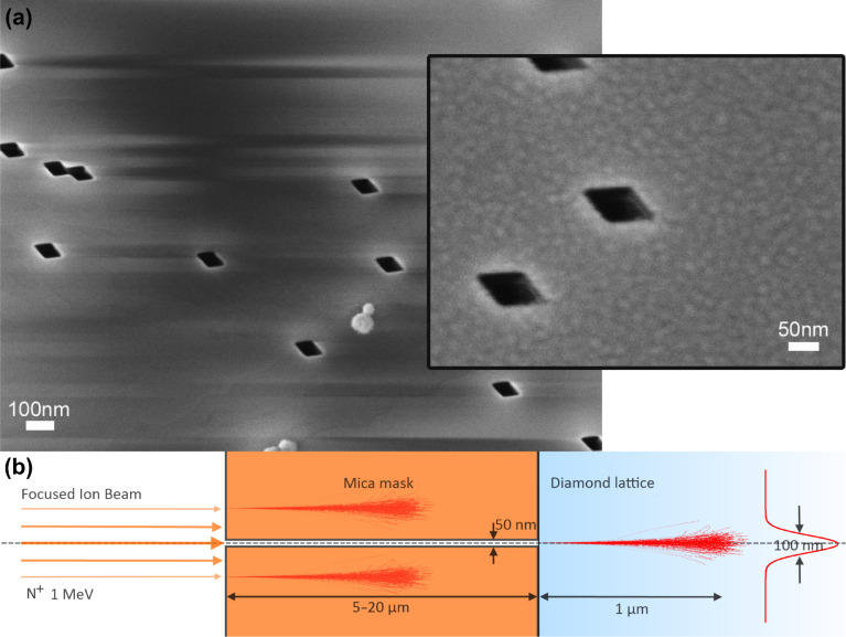
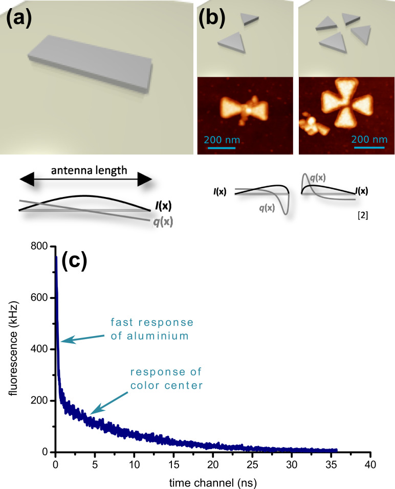
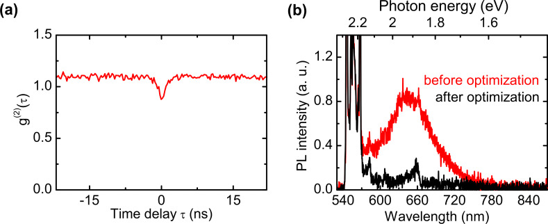
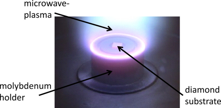
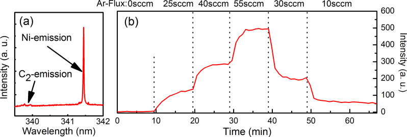
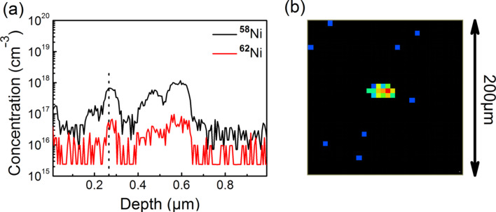
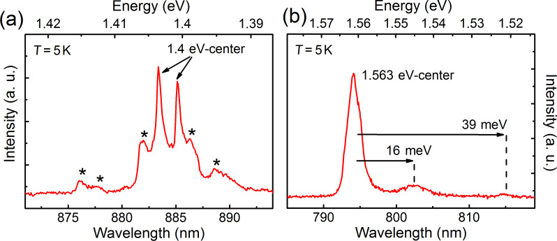
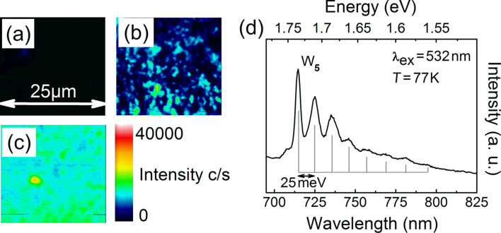
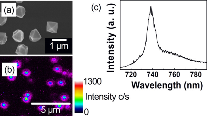
We demonstrate the coupling of single color centers in diamond to plasmonic and dielectric photonic structures to realize novel nanophotonic devices. Nanometer spatial control in the creation of single color centers in diamond is achieved by implantation of nitrogen atoms through high-aspect-ratio channels in a mica mask. Enhanced broadband single-photon emission is demonstrated by coupling nitrogen-vacancy centers to plasmonic resonators, such as metallic nanoantennas. Improved photon-collection efficiency and directed emission is demonstrated by solid immersion lenses and micropillar cavities. Thereafter, the coupling of diamond nanocrystals to the guided modes of micropillar resonators is discussed along with experimental results. Finally, we present a gas-phase-doping approach to incorporate color centers based on nickel and tungsten, in situ into diamond using microwave-plasma-enhanced chemical vapor deposition. The fabrication of silicon-vacancy centers in nanodiamonds by microwave-plasma-enhanced chemical vapor deposition is discussed in addition.

Keywords: CVD diamond doping; NV center; diamond; nanophotonics; plasmonic resonator; solid immersion lens.


Figures

Figure 1
Figure 1
(a) Scanning electron micrograph of a mica mask. High aspect ratio channels were created by bombardment with 1.6 GeV samarium ions. The channels appear as dark parallelograms. The inset shows the dimensions of an individual ion channel. (b) SRIM simulation of the ion implantation process through the mica mask. The thickness of the mica mask is chosen in the range 5–20 μm, such that the nitrogen ions (N+) are effectively stopped by the mask. The ions entering the channel create an implanted ion spot with a FWHM of about 100 nm, limited by straggle.
Figure 2
Figure 2
Nonlinear optical microscopy of implanted color centers by using ground-state-depletion microscopy mode. (a) Images of a color center obtained with increasing depletion laser power. (b) Measured optical resolution as a function of laser power. The solid line shows a theoretical fit for the achievable resolution formula image
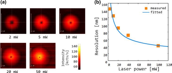
, where c is a proportionality constant, P is the optical power and r represents the maximum achievable resolution at infinite power, which is determined by technical limitations such as imperfections of the optical mode [6].
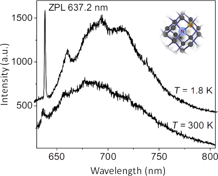
Figure 3
Figure 3
Fluorescence spectra of the nitrogen–vacancy defect in diamond. The upper curve shows the spectrum at liquid-helium temperature, the lower curve shows the spectrum at room temperature. The peak at a wavelength of 637.2 nm corresponds to the resonant optical transition (ZPL). The broad band at longer wavelength corresponds to phonon-broadened emission. The inset shows the molecular structure of the NV center in diamond consisting of a substitutional nitrogen atom with an adjacent vacancy.
Figure 4
Figure 4
Plasmonic resonator geometries, field I and current q for (a) half-wave antenna, (b) bow tie and crossed bow tie structure along with AFM images of the devices with embedded nanodiamond color center. (c) Fluorescence lifetime measurement of the coupled color center. A double exponential decay is observed. The initial fast decay is due to aluminium interband transitions and background. The second, slow decay is due to the coupled color center.
Figure 5
Figure 5
Enhancement of the collection efficiency with a hemispherical solid immersion lens (SIL). (a) Reduction of the effective numerical aperture due to refraction at the surface of a high-index medium. (b) Elimination of refraction with a hemispherical lens. (c) Collection efficiency as a function of numerical aperture with (red line) and without (black line) the solid immersion lens. Reproduced with permission from [10]. Copyright 2010 American Institute of Physics.
Figure 6
Figure 6
Macroscopic solid immersion lens [10]. (a) Photograph of a single crystalline diamond hemisphere. (b) Confocal fluorescence image of the focus plane. The bright spot in the center corresponds to a single nitrogen–vacancy defect. (c) Fluorescence emission spectrum. The peak at a wavelength of 637 nm (ZPL) corresponds to the resonant optical emission of the NV center. (d) Photon antibunching. The dip at time delay τ = 0 is well below 0.5, indicating a single quantum emitter. (e) Saturation curves with and without the solid immersion lens. Reproduced with permission from [10]. Copyright 2010 American Institute of Physics.
Figure 7
Figure 7
Fabrication of a microscopic diamond hemisphere by focused ion beam milling. (a) Grid of FIB markers for the precise alignment of the SIL on top of a single color center. (b) Fluorescence microscope image of one quadrant of FIB markers. The bright blue spots are single color centers. A color center a few microns below the surface (not visible in this image) is selected as the target emitter. Note that the image distortion between subsequent scan lines is caused by bi-directional motion of the imaging piezo scanner. (c) SEM image of a microscopic SIL. The complete FIB process takes approximately 30 min.
Figure 8
Figure 8
(a) Scanning electron microscopy (SEM) image of a micropillar resonator with embedded diamond nanocrystals in the central spacer layer. (b) Transmission electron microscopy (TEM) image of diamond nanocrystals. The average size of the nanodiamonds is 20 nm. (c–e) Mode spectrum of a pillar microcavity (2.9 µm diameter) with an ensemble of diamond nanocrystals in the spacer layer. (c) Simulated spatial cavity modes. (d) Spatio-spectrally resolved photoluminescence emission and (e) white-light transmission spectrum. Calculated spectral mode positions are indicated by vertical grey lines.
Figure 9
Figure 9
(a) Normalized intensity autocorrelation function g(2)(τ) from a micropillar cavity of 1.6 µm diameter with embedded diamond nanocrystals. (b) Comparison between the photoluminescence emission from a standard (black) and an optimized (red) sputtered SiO2 layer.
Figure 10
Figure 10
View into the MWPECVD reactor during growth of a single-crystalline diamond layer.
Figure 11
Figure 11
(a) Optical emission spectroscopy: observed nickel emission in the MWPECVD plasma during diamond growth with addition of nickelocene. (b) Temporal evolution of the nickel emission (341.47 nm line) during MWPECVD diamond growth altering the argon/nickelocene addition. The intensity of the nickel emission is solely determined by the carrier gas flux to the reactor. Furthermore, the nickel emission is steady for constant nickelocene additions thereby demonstrating the reproducibility of the utilized gas-phase-doping approach. Reproduced with permission of the author from [25].
Figure 12
Figure 12
(a) SIMS depth profile of nickel-doped single-crystal diamond layer. The intensity of the two “marker” isotopes 58Ni and 62Ni is in accordance with the known natural abundance, thereby verifying nickel incorporation. (b) SIMS-signal from picture (a) observed at a depth of 0.25 µm. The nickel signal emanates from a spot indicating the formation of nickel clusters during diamond growth with simultaneous nickelocene addition. Reproduced with permission of the author from [25].
Figure 13
Figure 13
Cathodoluminescence spectra measured at a temperature of 5 K on a nickel-doped single-crystal diamond layer. (a) Emission lines of the 1.4 eV center at 883.4 nm and 885.1 nm, verifying nickel incorporation. Origins of accompanying lines marked with an asterisk are unknown. (b) Luminescence of the 1.563 eV center (“NE8-defect”) observed in the same diamond layer. Reproduced with permission of the author from [25].
Figure 14
Figure 14
(a–c) Room-temperature PL mapping excited at a wavelength of 660 nm on (111) diamond layers grown by MWPECVD with different additions of W(CO)6: (a) no addition (reference layer); (b) with a mole fraction of 1.1 × 10⁻⁶ W(CO)6 in the process gas; (c) with a mole fraction of 1 × 10⁻⁵ W(CO)6 in the process gas. (d) Photoluminescence spectrum obtained from a tungsten-doped single-crystal diamond layer; acquired at 77 K with 532 nm laser excitation. The tungsten-related W5-luminescence at a wavelength of 714 nm together with several pronounced phonon sidebands is visible. Reproduced with permission of the author from [25].
Figure 15
Figure 15
(a) As-grown nanodiamond particles on a silicon substrate. (b) Confocal photoluminescence mapping (660 nm excitation wavelength), recorded at room temperature. The integrated intensity emitted in the spectral window between 725 and 755 nm was measured. Bright areas in the scan correlate with nanodiamond particles. (c) Spectrally resolved PL emission from a particle in (b). The SiV luminescence verifies the successful incorporation of silicon during growth.

References

    1. Hwang J, Pototschnig M, Lettow R, Zumofen G, Renn A, Götzinger S, Sandoghdar V. Nature. 2009;460:76–80. doi: 10.1038/nature08134. - DOI - PubMed
    1. Hedges M P, Longdell J J, Li Y, Sellars M J. Nature. 2010;465:1052–1056. doi: 10.1038/nature09081. - DOI - PubMed
    1. Kurtsiefer C, Mayer S, Zarda P, Weinfurter H. Phys Rev Lett. 2000;85:290–293. doi: 10.1103/PhysRevLett.85.290. - DOI - PubMed
    1. Pezzagna S, Rogalla D, Becker H-W, Jakobi I, Dolde F, Naydenov B, Wrachtrup J, Jelezko F, Trautmann C, Meijer J. Phys Status Solidi A. 2011;208:2017–2022. doi: 10.1002/pssa.201100455. - DOI
    1. Ziegler J F. The Stopping and Range of Ions in Matter. 2012 Available from: http://www.srim.org/

LinkOut - more resources