. 2013 Nov 13;13(11):4999-5005.
doi: 10.1021/nl304602d. Epub 2013 Feb 14.

Single-cell photonic nanocavity probes

Affiliations

Single-cell photonic nanocavity probes

Gary Shambat et al. Nano Lett. .

Abstract

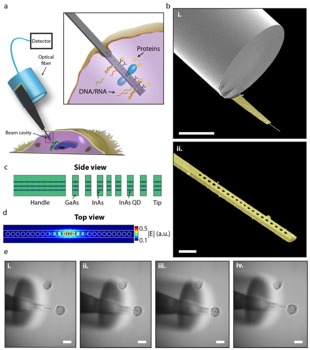
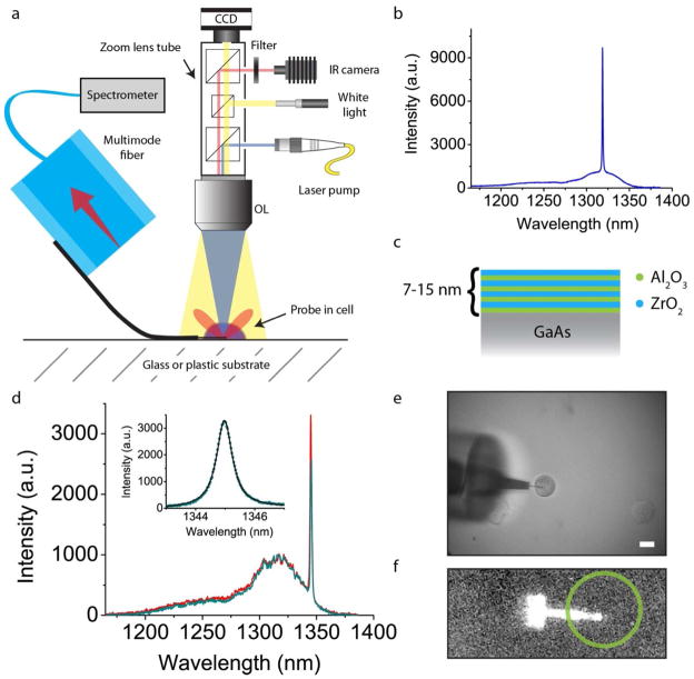
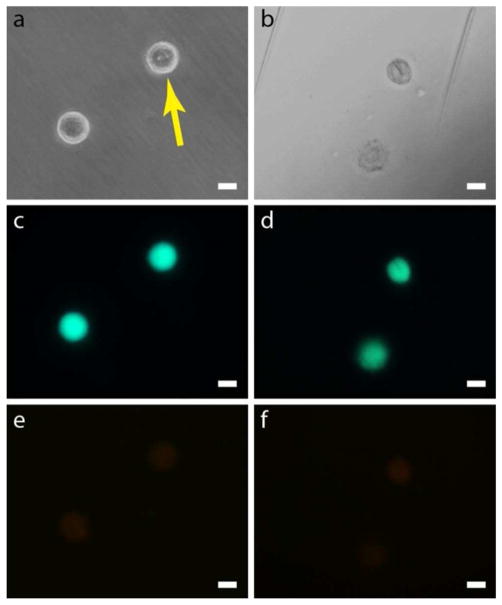
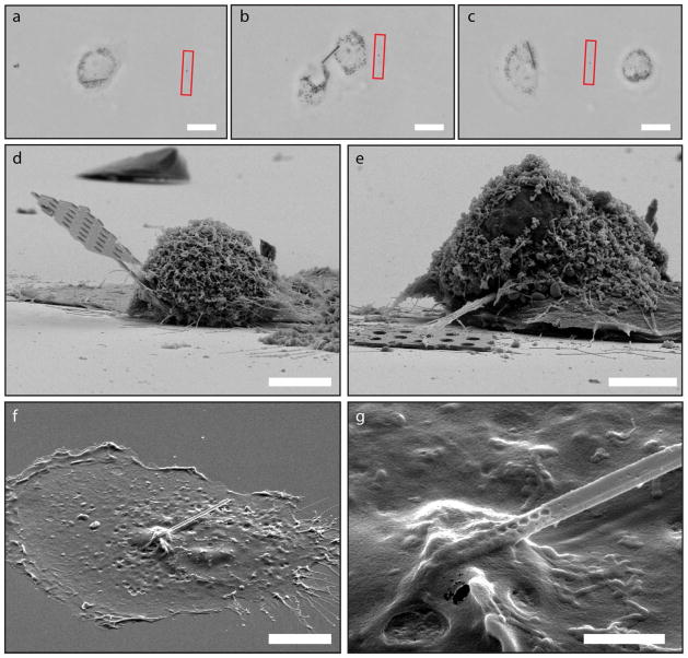
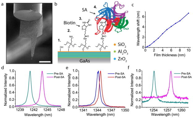
In this report, we demonstrate for the first time photonic nanocavities operating inside single biological cells. Here we develop a nanobeam photonic crystal (PC) cavity as an advanced cellular nanoprobe, active in nature, and configurable to provide a multitude of actions for both intracellular sensing and control. Our semiconductor nanocavity probes emit photoluminescence (PL) from embedded quantum dots (QD) and sustain high quality resonant photonic modes inside cells. The probes are shown to be minimally cytotoxic to cells from viability studies, and the beams can be loaded in cells and tracked for days at a time, with cells undergoing regular division with the beams. We present in vitro label-free protein sensing with our probes to detect streptavidin as a path towards real-time biomarker and biomolecule detection inside single cells. The results of this work will enable new areas of research merging the strengths of photonic nanocavities with fundamental cell biology.


Figures

Figure 1
Figure 1
Photonic nanoprobe design and single cell interrogation. a, Schematic of photonic crystal nanobeam probe for single-cell investigation. The nanobeam cavity extends from a larger semiconductor template which is mounted on the side edge of a multimode optical fiber. The inset corresponds to the box in the main figure depicting potential sensing modalities of the cavity such as label-free protein or DNA/RNA detection. b, Angled scanning electron microscope (SEM) pictures of a typical fabricated device (in false-color). The ripple on the fiber facet is a small fracture from the fiber cleaver. A close-up of the beam portion is shown in b(ii). Some light debris from the sputter coating is also visible. The striations on the side of the beam are the three wetting layers of the self-assembled quantum dots. c, Schematic of the MBE material stack. The background material is GaAs and the quantum dots (shown as triangles) are InAs inside an InAs wetting layer. d, Finite-difference time domain simulation picture of the electric field magnitude of the fundamental cavity mode for this photonic structure. e, Sequence of bright-field images of a nanocavity probe penetrating a single PC3 cell, viewed from above. The probe is first positioned outside the cell with the membrane flexed and flush against the petri dish substrate. It is then maneuvered into the side of the cell and finally retracted. The optical fiber, which is positioned higher than the membrane is seen defocused in the pictures. Scale bars: 50 μm (b(i)), 1 μm (b(ii)), 20 μm (e).
Figure 2
Figure 2
Optical characterization of photonic crystal cavities inside single cells. a, Diagram of the optical setup used in the experiment. A three-axis micromanipulator positions the probe such that the GaAs membrane (shown in black) flexes and rests against the substrate. A zoom lens tube contains beam splitters for laser pump and white light illumination, as well as image capture. OL is objective lens. Not shown is the liquid level, which submerges the optical fiber but does not reach the objective lens. b, PL spectrum of a single nanoprobe cavity measured in air. The QD emission uncoupled to the cavity is the small background spreading from 1,150 nm to 1,350 nm and the cavity mode is the sharp peak at 1,319 nm. c, Illustration of the alumina/zirconia nanolaminate used to coat the entire device, protecting it from photo-induced oxidation. Stacks alternated between 1 nm and 2 nm per layer thicknesses, and total stack thicknesses of 7–15 nm. d, PL spectrum of the same cavity from b now in a cell (teal) and its surrounding medium (red). There is negligible wavelength difference between the two spectra; however the collection intensity inside the cell (teal) is slightly lower, likely due to scattering from the plasma membrane. Inset shows a close-up of the cavity mode which has a Q-factor of 2,200. e, Corresponding white light image of the probe and cell for which data in d were taken. f, Corresponding IR image of the probe’s QD emission and a circular outline of the approximate cell location. Scale bar, 20 μm.
Figure 3
Figure 3
Short-term cell viability results. a, Phase contrast image of two cells, one of which was poked by a nanoprobe (shown by the arrow) and one which was left untouched. b, Bright field image of two different cells, one which was loaded with a nanobeam and one which was left untouched. The nanobeam is the clear dark line in the upper cell. The cells look different compared to a because the microscope settings were changed to better visualize the cell interior. Also, the two parallel streaks are reference marks scratched into the petri dish with a metal probe to locate the treated cell. c, d, Green fluorescence from the calcein viability dye for the corresponding cells pictured in a and b. All cells show similar levels of green fluorescence intensity indicating the viability of both poked and loaded cells. In d it is even possible to see the outline of the loaded beam in the cell by an absence of color. e, f, Red fluorescence from the ethidium homodimer viability dye for the corresponding cells picture in a and b. The emission is very weak and uniform across all cells indicating the cell membranes were not compromised. Scale bars, 20 μm.
Figure 4
Figure 4
Nanobeam cell division and SEM images of loaded cells. a–c, Bright field images of a loaded cell prior (a), during (b), and after (c) cell division. Images were taken 30, 42, and 46 hours after loading the cell with the nanobeam, respectively. The red box indicated the position of the original scratch mark created during beam loading. This provides a reference mark for seeing how far the cells have migrated, which we observed to be up to 250 μm during the tracking period. d, SEM image of a nanobeam probe including part of the handle tip lodged inside a typical cell. A few flatter cells are seen in the background. e, SEM image of another cell pierced by a nanobeam with connected handle tip. f, SEM image of a cell that has only a beam inserted. This cell was not critical point dried and therefore is much flatter than the cells in d–e. g, Close-up of the entry point of the nanobeam into the cell in f. The holes that make up the cavity are clearly seen as they transition from fully visible outside of the cell to being hidden under the cell membrane. Scale bars: 20 μm (a–c), 5 μm (d–e), 10 μm (f), 2 μm (g).
Figure 5
Figure 5
Nanoprobe detection of Streptavidin binding. a, SEM image of a modified nanoprobe that has extended ‘wings’ meant to wrap around the edge of the optical fiber, thus preventing sticking. b, Illustration of the surface chemistry for protein detection. The original, nanolaminate-coated GaAs, is coated with an additional layer of silica which has terminal hydroxyl groups. Aminosilanization with APTES yields an amine-terminated surface to which biotin binds. Finally Streptavidin specifically binds to the surface biotin molecules. c, Finite-difference frequency domain (FDFD) simulation of the expected wavelength shift as the organic film thickness is increased. The film was modeled as a uniform layer of refractive index equal to 1.45. d, Spectra of a chip-bound nanobeam both before and after SA adsorption, demonstrating a clear and large redshift of the cavity peak. e, Non-specific binding of a different beam cavity shows a much smaller redshift of 0.5 nm. f, Spectra of a nanoprobe device (shown in 5a) for the same specific binding chemistry. As in d, the redshift is clear and large. The difference in background PL is due to slightly different focus conditions of the laser spot, however, this has no bearing on the wavelength information. Scale bar, 50 μm.

References

    1. Xie C, Lin Z, Hanson L, Cui Y, Cui B. Nature Nanotech. 2012;7:185–190. doi: 10.1038/nnano.2012.8. - DOI - PMC - PubMed
    1. Duan X, et al. Nature Nanotech. 2011;7:174–179. doi: 10.1038/nnano.2011.223. - DOI - PMC - PubMed
    1. Singhal R, et al. Nature Nanotech. 2011;6:57–64. doi: 10.1038/nnano.2010.241. - DOI - PubMed
    1. Yum K, Na S, Xiang Y, Wang N, Yu M-F. Nano Lett. 2009;9:2193–2198. doi: 10.1021/nl901047u. - DOI - PMC - PubMed
    1. VanDersarl JJ, Xu AM, Melosh NA. Nano Lett. 2012;12:3881–3886. doi: 10.1021/nl204051v. - DOI - PubMed

Publication types

Substances

LinkOut - more resources