. 2013:3:1248.
doi: 10.1038/srep01248. Epub 2013 Feb 13.

Tunable transport gap in narrow bilayer graphene nanoribbons

Affiliations

Tunable transport gap in narrow bilayer graphene nanoribbons

Woo Jong Yu et al. Sci Rep. 2013.

Abstract

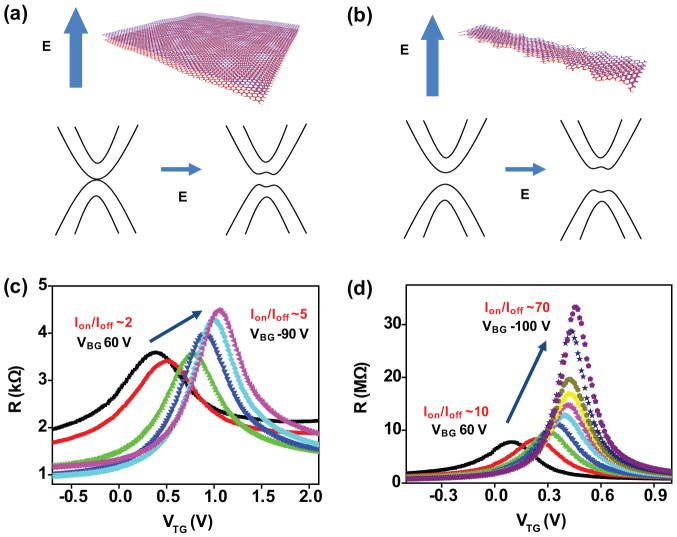
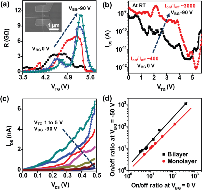
The lack of a bandgap makes bulk graphene unsuitable for room temperature transistors with a sufficient on/off current ratio. Lateral constriction of charge carriers in graphene nanostructures or vertical inversion symmetry breaking in bilayer graphene are two potential strategies to mitigate this challenge, but each alone is insufficient to consistently achieve a large enough on/off ratio (e.g. > 1000) for typical logic applications. Herein we report the combination of lateral carrier constriction and vertical inversion symmetry breaking in bilayer graphene nanoribbons (GNRs) to tune their transport gaps and improve the on/off ratio. Our studies demonstrate that the on/off current ratio of bilayer GNRs can be systematically increased upon applying a vertical electric field, to achieve a largest on/off current ratio over 3000 at room temperature.


Figures

Figure 1
Figure 1. Schematic illustration of the fabrication procedures to obtain dual-gated bilayer graphene nanoribbon FET.
(a), Si/Al2O3 core/shell nanowires are transferred onto a bilayer graphene sheet. (b), Source and drain electrodes are formed on aligned bilayer graphene and Si/Al2O3 core/shell nanowires. (c), Uncovered bilayer graphene is etched by oxygen plasma, and bilayer graphene nanoribbons are produced underneath Si nanowires. (d), A thin film of 60 nm HfO2 is deposited by e-beam evaporation to prevent electrical breakdown of plasma damaged SiO2. (e), Top gate electrode is deposited as a final process. (f), Schematic of the cross-sectional view of the device.
Figure 2
Figure 2. The opening of transport gap in bilayer graphene by narrowing channel width.
(a–b), Schematic images of (a), bilayer graphene sheet and (b), bilayer graphene nanoribbon with corresponding band diagrams. (c), Transfer characteristics of a bilayer GNR FET at the various oxygen plasma etching time (VDS = 0.1 V). The etching time was varied from 0 s to 240 s from top to bottom in steps of 60 s.
Figure 3
Figure 3. The further opening of transport gap in bilayer graphene nanoribbon by breaking the inversion symmetry.
(a–b), Schematic images of (a), bilayer graphene sheet and (b), bilayer graphene nanoribbon with a vertical electrical displacement field and corresponding energy band structure before and after applying the displacement field. (c), Switching behavior of a bilayer graphene sheet FET at VDS = 0.1 V and VBG varied from 60 to −90 V in steps of 30 V. (d), Switching behavior of a bilayer graphene nanoribbon FETs at VDS = 0.1 V and VBG varied from 60 to −100 V in steps of 20 V.
Figure 4
Figure 4. High on/off ratio bilayer graphene nanoribbon FET.
(a–b), The room temperature (a), switching behavior and (b), transfer characteristics of the narrow bilayer graphene nanoribbon FET at the various back gate voltages (VDS = 10 mV). VBG was modulated from 0 to −90 V in steps of 30 V. Inset in (a) shows SEM image of the bilayer graphene nanoribbon FET used in this measurement. (c), IDS-VDS output characteristics of the narrow bilayer graphene nanoribbon FET with VTG varied from 1 to 5 V in steps of 0.5 V (VBG = −90 V). (d), Relations between the on/off current ratio of monolayer and bilayer GNR FETs before and after application of the vertical electric field. The vertical and horizontal axes indicate that the on/off current ratio before and after the application of the vertical electric field.

Similar articles

Cited by

References

    1. Novoselov K. S. et al. Electric field effect in atomically thin carbon films. Science 306, 666–669 (2004). - PubMed
    1. Novoselov K. S. et al. Two-dimensional gas of massless Dirac fermions in graphene. Nature 438, 197–200 (2005). - PubMed
    1. Dean C. R. et al. Boron nitride substrates for high-quality graphene electronics. Nat. Nanotechnol 5, 722–726 (2010). - PubMed
    1. Wu Y. Q. et al. High-frequency, scaled graphene transistors on diamond-like carbon. Nature 472, 74–78 (2011). - PubMed
    1. Liao L. et al. High-speed graphene transistors with a self-aligned nanowire gate. Nature 467, 305–308 (2010). - PMC - PubMed

Publication types