

Review
doi: 10.1021/cr300337x.
Epub 2013 Feb 14.
Advances in microfluidic materials, functions, integration, and applications
Affiliations
- PMID: 23410114
- PMCID: PMC3624029
- DOI: 10.1021/cr300337x
Item in Clipboard
Review
Advances in microfluidic materials, functions, integration, and applications
Chem Rev.
.
No abstract available
Figures

Microcantilevers (a–e) and a microring resonator (f) made from silicon. (a) Schematic diagram of waveguides and microcantilever array layout on die. (b) Optical image of two microcantilevers in a fabricated array. (c) Close up scanning electron micrograph (SEM) image of the unclamped end of a microcantilever (left of 165 nm gap) and the differential splitter capture waveguide (right of gap). (d) Photograph of complete integrated device showing the fluid microchannels (red) and control valves (green). (e) Cross-section of fluid microchannel at a microcantilever array. (f) Top-view SEM image of a microring resonator and linear waveguide, visible through an annular opening in the fluoropolymer cladding layer. Reprinted with permission from refs. and . Copyright 2009, American Chemical Society and 2011, The Royal Society of Chemistry.

Silicon nanowire system for cardiac biomarker detection. (a) Image of silicon nanowire (SiNW) device array chip, integrated with microfluidic system for fluid exchange. Fluids are deposited into the acrylic well through the inflow tube on the left (red arrow) and removed from the outflow tube on the right (blue arrow). (b) Schematic showing the layout of the SiNW device array on the chip. A total of 36 clusters of 5 nanowires each were available for use. (c) SEM image of a cluster of nanowires. Each nanowire is individually addressable by oxide-passivated metal contact lines running out to the edge of the chip. Reprinted with permission from ref. . Copyright 2009, American Chemical Society.

Microfluidic valve network. Photograph of the multiplexed latching valve test device, with a four-bit demultiplexer (top box) for routing pressure and vacuum pulses from the single “input” connection to each of sixteen latching valves (bottom box). Reprinted with permission from ref. . Copyright 2006, The Royal Society of Chemistry.

μCE nanospray glass device. Schematic diagrams of (a) short- and (b) long-channel μCE-ESI-MS chips. The length of the separation channel was 4.7 cm in (a) and 20.5 cm in (b). The reservoirs are labeled S (sample), B (buffer), SW (sample waste), and SC (side channel). The direction of EOF is indicated by the arrows in (a). (c) CCD image of the electrospray plume generated from the corner of a μCE-ESI-MS chip. Reprinted with permission from ref. . Copyright 2008, American Chemical Society.
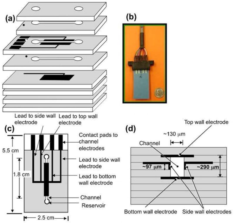
Microfluidic device made from LTCC. (a) Multilayer stacking to create a screen-printed gold/LTCC microchannel device. (b) Photograph of a microchannel device with an edge connector. (c) Top down view of a device. (d) Cross-section view of the microchannel showing the four gold electrodes. The width of the chip in (d) is not drawn to scale. Reprinted with permission from ref. . Copyright 2010, Springer.

Large scale integrated PDMS microfluidic valve network. (Top) open and (middle) closed 8 × 8 and 6 × 6 μm2 valves. (Bottom) demonstration of geometry dependent valving; the flow channel on the left is closed while the one on the right remains open when the control channel width is 4 μm. Reprinted with permission from ref. . Copyright 2012, The Royal Society of Chemistry.

Dyneon THV, a perfluorinated polymer used for droplet microfluidics. (a) Droplet production in a flow focusing device (typical volumes ~10 pL) and plug production in a T-junction (typical volumes ~100 nL). (b) Transmission and fluorescence images of a plug train circulating in a serpentine microchannel. Water solution contains 0.4 ng/mL of DNA labeled with SYBR Green I. (c) Fluorescence intensity collected over time in the center of a channel. Each peak corresponds to the passage of a plug, and the intensity is proportional to the DNA concentration. (d) Image of the whole chip. Reprinted with permission from ref. . Copyright 2011, The Royal Society of Chemistry.

PS microfluidic devices. Images of (a) epoxy molds, (b) through-hole embossed PS parts, and (c) bonded devices applied in neutrophil chemotaxis and nonadherent multiple myeloma cell immunostaining. Reprinted with permission from ref. . Copyright 2011, American Chemical Society.

Poly-PEGDA microfluidics. (a) Structure of poly-PEGDA. (b) Side-view schematic of a poly-PEGDA device. (c) Bottom-view photograph of a finished poly-PEGDA device; white bar is 0.5 cm. (d) Fluorescence comparison of PDMS and poly-PEGDA over time during flow of a dilute, adsorptive, fluorescently labeled protein solution. (e) μCE of amino acids (top) and proteins (bottom) using a poly-PEGDA microchip. Reprinted with permission from ref. . Copyright 2011, American Chemical Society.

Solvent-resistance and antifouling properties of an all-Teflon microfluidic device. (a) A PFA chip with microchannels filled with acetone (colored with a red dye) and DMSO (colored with a blue dye). (b) Laminar flow of dyed organic solvents in an all-Teflon chip. (c) Fluorescence images of different kinds of microchannels filled with a 100 μg/mL GFP aqueous solution. (d) Fluorescence images of the channels in (c) after washing with buffer for 1 min. Reprinted with permission from ref. . Copyright 2011, National Academy of Sciences.

Zein-glass microfluidic devices with complex fluidic pathways. (a) Interconnected letters composed of continuous microfluidic channels, (b) a microfluidic network with channels and chambers, and (c) a solved microfluidic maize maze with multiple false paths. Blue food dye was used for visualization. All scale bars are 5 mm. Reprinted with permission from ref. . Copyright 2011, The Royal Society of Chemistry.

SU8 microfluidic device with check valves. (a) Cantilever-based diaphragm micropump. (b) Image of the cantilever in (i) open mode and (ii) closed mode. Reprinted with permission from ref. . Copyright 2011, The Royal Society of Chemistry.

3-D origami paper microfluidic device. (a) Chromatography paper having photolithographically patterned channels, reservoirs, and a folding frame. (b) Top layer of the folded paper revealing four inlet reservoirs in the center of the device (four flanking circular features are present within the 3-D structure but are visible due to the transparency of the paper). (c) Bottom layer of the folded paper. (d) The aluminum housing used to support the 3-D paper microfluidic system. (e) An unfolded, nine-layer paper microfluidic device after injecting four aqueous, colored solutions through the four injection ports. Reprinted with permission from ref. . Copyright 2011, American Chemical Society.

(a) Schematic of the microfluidic aptasensor. (b) Cross-sectional view along line A–A in (a), illustrating the layered structure. (c) Photograph of a packaged device. Reprinted with permission from ref. . Copyright 2011, Elsevier.

Schematic illustration of chip architecture and operation. (A) Chip is loaded with trailing and leading buffers surrounding the sample by applying vacuum to wells 4 and 5. (B) ITP stacking is initiated by applying an electric field between wells 1 and 7. (C) When the stacked sample reaches the junction for ITP-gel electrophoresis handoff, the cathode is switched from well 1 to well 6. (D) Gel electrophoresis separation. (E) Typical electropherogram obtained after preconcentration, I is the fluorescence intensity and S is the peak separation. Reprinted with permission from ref . Copyright 2008, American Chemical Society.

Photograph of a microfluidic device and zoom view of a preconcentration membrane. (A) Photograph of a microfluidic device used for sample preconcentration. Reservoir labels are 1, sample; 2, sample waste; and 3–6, buffer. (B) Photomicrograph of microchannel intersection region showing position of the polymerized membrane. Reprinted with permission from ref. . Copyright 2011, Wiley.

Layout of a microfluidic chip used for enzyme analysis. RR, SR, BR, and WR represent reagent reservoir, sample reservoir, buffer reservoir, and waste reservoir, respectively. Reprinted with permission from ref. . Copyright 2010, American Chemical Society.

Microchip liquid chromatography with a monolithic column. (A) Chip design and (B) experimental system with dynamic sample injection. (C) Chip design and (D) experimental system for online sample cleanup and enrichment-HPLC separations. Reprinted with permission from ref. . Copyright 2009, American Chemical Society.

Schematic of a microfluidic device with serpentine channel for N-glycan analysis. Inset –image of an asymmetrically tapered, 180° turn. Reprinted with permission from ref. . Copyright 2012, American Chemical Society.

Flow process for multilayer PMMA microfluidic device fabrication. (a–c) Laser cutting of openings for reservoirs (larger) and interlayer through-holes (smaller). (d–f) Hot embossing of the bottom layer (upper surface) and the top layer (lower surface). (g) Assembly of the middle and bottom layers through thermal bonding. (h) A completed device with top layer thermally bonded to the assembly in (g). Reservoirs 1–8 are sample inlets for different analytes. Reservoir 9 is the fluorescent label inlet. Reservoirs 10–12 are buffer inlet, injection waste, and waste, respectively. Reprinted with permission from ref. . Copyright 2011, American Chemical Society.

(A) Photograph of an on-chip UV detection microdevice. (B) SEM image of a chip showing a cross-sectional view of the detection cell to the left and a waveguide to the right. (C) Sketch of channel and waveguide layout. (D) Schematic illustration of the setup. Reprinted with permission from ref. . Copyright 2009, Wiley.

Layout of (A) a hybrid PDMS/glass contactless conductivity detection microchip and (B) a similar chip that also offers amperometric detection. WE: working electrode; RE: reference electrode; CE: counter electrode. Reprinted with permission from ref. . Copyright 2010, The Royal Society of Chemistry.

Microfluidic eductor operation. (A) Schematic representation of the educator, illustrating the configuration of the transfer capillary, ESI needle, and gas nozzle, coupled to a closed droplet microfluidic device. Reprinted with permission from ref. . Copyright 2012, American Chemical Society.

A) Schematic representation of a microspike based skin patch for glucose/lactate detection. B) Schematic representation of a microfluidics based system to study mass transport phenomena in biosensors. Reprinted with permission from ref. . Copyright 2012, The Royal Society of Chemistry.

Schematic diagram of microchip fabrication. (a) Thermal and pressure bonding of the device sandwiching two silica capillaries and an SU-8 ESI emitter. (b) Hot embossing of COC against the silicon master engraved by reactive ion etching. (c) Gold–titanium electrode deposition for electrochemical pumping and ESI. Reprinted with permission from ref. . Copyright 2008, Springer.

Illustration of microchip design and fabrication. (A) Design of the microchip including flow channel (solid line) and control channel (dashed line). (B) Schematic of microchip fabrication. (a) Flow layer containing the sample injection and separation channels. (b) Control layer containing the valving channel on a thin PDMS film. (c) Unpatterned bottom layer to enclose the control channel. (C) Template for flow layer fabricated with positive photoresist. (D) Template for control layer fabricated with SU-8. (E) Photograph of the final PDMS microchip. (F) Photograph of the T intersection assembled with a pneumatic valve. Reprinted with permission from ref. . Copyright 2011, Wiley.

Geometry of three-dimensional serpentine mixing channel. Reprinted with permission from ref. . Copyright 2009, Elsevier.

Microdialysis sampling integrated with microfluidics. (A) Schematic of bilayer microchip with a picture of the valving interface between the hydrodynamic flow and electrophoretic flow. Abbreviations: B, buffer; BW, buffer waste; PB, pushback; SW, sample waste; S, sample; NO, normally open; NC, normally closed. (B) Picture taken on gray background showing how the microdialysis tubing, access pins, and voltage leads are inserted into the microchip. (C) Coupling of the microchip device with microdialysis sampling, associated tubing, and syringe pump. Reprinted with permission from ref. . Copyright 2008, American Chemical Society.
Layout of an integrated affinity extraction-μCE microdevice. (a) Schematic diagram and (b) photograph of a typical microchip with integrated affinity column. Reprinted with permission from ref. . Copyright 2010, The Royal Society of Chemistry.

Droplet compartmentalization of the components of a mixture separated by μCE. a) Schematic representation of the general method used for the compartmentalization of the separated bands in droplets. b) Schematic representation of the fluidic design used to integrate μCE with droplet compartmentalization. c) Droplet-formation region shown in detail. Reprinted with permission from ref. . Copyright 2009, Wiley.

Microchip blood analysis system. (a) Scheme depicting plasma separation from a finger prick of blood by harnessing the Zweifach-Fung effect. Multiple DNA-encoded antibody barcode arrays are patterned within the plasma-skimming channels for in situ protein measurements. (b) Antibody arrays patterned in plasma channels for in situ protein measurement. A–C indicate different DNA codes. (1)–(5) denote DNA-antibody conjugate, plasma protein, biotin-labeled detection antibody, streptavidin-Cy5 fluorescence probe and complementary DNA-Cy3 reference probe, respectively. The inset represents a barcode of protein biomarkers, which is read out using fluorescence detection. Reprinted with permission from ref. . Copyright 2008, Nature Publishing Group.

Schematic of an affinity capture microfluidic device. (a) Side view. Cell mixtures are loaded into the chip, where nontarget cells are captured and target cells pass through for collection. (b) Image of an experimental device. Red food coloring was introduced into channels to help with visualization. Reprinted with permission from ref. . Copyright 2011, American Chemical Society.

Assay overview. (A) Template DNA is added to a PCR reagent mixture containing phosphorylated reverse primers. (B) The template is PCR amplified. (C and D) Lambda exonuclease is mixed with the product and digests the phosphorylated strands. (E) Prior to electrochemical analysis in the detection chamber, MgCl2 is added to adjust the salt concentration from 1.5 mM to 50 mM for hybridization. (F) Before introducing sample to the sensor, a baseline redox current is measured. Next, the ssDNA product hybridizes with the E-DNA probe modulating the redox current signal. Finally, the E-DNA probe is regenerated to verify the hybridization event. Reprinted with permission from ref. . Copyright 2009, American Chemical Society.

(A) Photograph of a microfluidic chip, enhanced to highlight the channels. (B) A microscopic view of the reactor well entrance with immobilized pepsin beads. Arrows indicate direction of flow. (C) A schematic depiction of the reactor well, side view. Single-headed arrows indicate direction of flow. Reprinted with permission from ref. . Copyright 2010, Wiley.

a) Schematic of the aerosol μCE system, showing growth tube collector, water reservoir for passive wetting of the wick, and the microchip into which the aerosols are deposited. All dimensions are in millimeters. b) Exploded view of the microchip design. The gray lines are platinum electrophoresis electrodes, the gold lines are gold-plated tungsten detection electrodes, the black lines are microchannels, the white circles are holes in the PDMS, and the gray circles show the locations where the holes in the adjacent layer are aligned. The chip is assembled bottom-to-top, layers 1–4. Reprinted with permission from ref. . Copyright 2009, American Chemical Society.
References
Publication types
MeSH terms
Substances
Grants and funding
LinkOut - more resources
Full Text Sources
Other Literature Sources
