

Sub-10 nm gate length graphene transistors: operating at terahertz frequencies with current saturation
- PMID: 23419782
- PMCID: PMC3575621
- DOI: 10.1038/srep01314
Sub-10 nm gate length graphene transistors: operating at terahertz frequencies with current saturation
Abstract
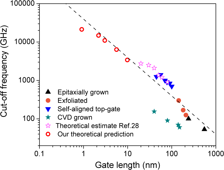
Radio-frequency application of graphene transistors is attracting much recent attention due to the high carrier mobility of graphene. The measured intrinsic cut-off frequency (f(T)) of graphene transistor generally increases with the reduced gate length (L(gate)) till L(gate) = 40 nm, and the maximum measured f(T) has reached 300 GHz. Using ab initio quantum transport simulation, we reveal for the first time that f(T) of a graphene transistor still increases with the reduced L(gate) when L(gate) scales down to a few nm and reaches astonishing a few tens of THz. We observe a clear drain current saturation when a band gap is opened in graphene, with the maximum intrinsic voltage gain increased by a factor of 20. Our simulation strongly suggests it is possible to design a graphene transistor with an extraordinary high f(T) and drain current saturation by continuously shortening L(gate) and opening a band gap.
Figures
 ,
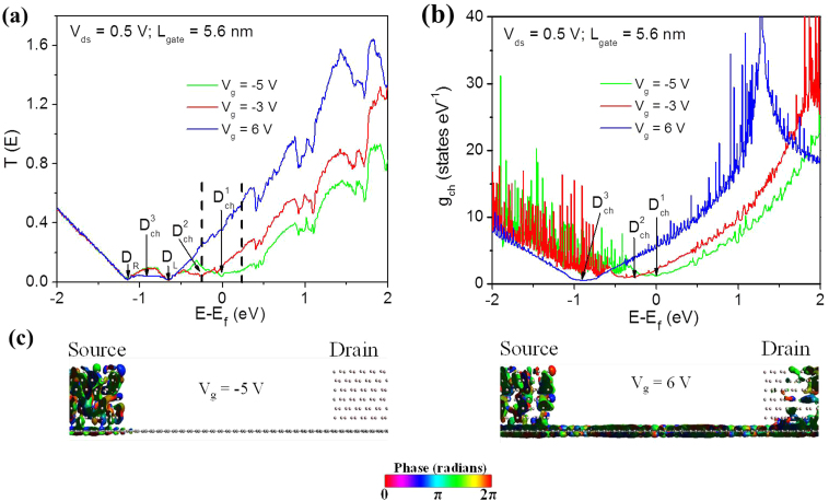
,  , and
, and  denote the Dirac point of the channel graphene under Vg = −5.0, −3.0, and 6.0 V, respectively. (b) Projected density of states on carbon atoms in the channel under Vg = −5.0, −3.0, and 6.0 V, respectively. (c) Transmission eigenstates of the off-state (Vg = −5.0 V) and on-state (Vg = 6.0 V) at Ef and k = (0.4, 0). The isovalue is 0.6 a.u.
References
-
- Novoselov K. S. et al. Two-dimensional gas of massless Dirac fermions in graphene. Nature 438, 197–200 (2005). - PubMed
-
- Zhang Y. B., Tan Y. W., Stormer H. L. & Kim P. Experimental observation of the quantum Hall effect and Berry's phase in graphene. Nature 438, 201–204 (2005). - PubMed
-
- Berger C. et al. Electronic confinement and coherence in patterned epitaxial graphene. Science 312, 1191–1196 (2006). - PubMed
-
- Geim A. K. & Novoselov K. S. The rise of graphene. Nat. Mater. 6, 183–191 (2007). - PubMed
-
- Avouris P. Graphene: electronic and photonic properties and devices. Nano Lett. 10, 4285–4294 (2010). - PubMed
Publication types
LinkOut - more resources
Full Text Sources
Other Literature Sources
Miscellaneous
