Fabricating nanogaps by nanoskiving
- PMID: 23711512
- PMCID: PMC3683935
- DOI: 10.3791/50406
Fabricating nanogaps by nanoskiving
Abstract
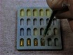
There are several methods of fabricating nanogaps with controlled spacings, but the precise control over the sub-nanometer spacing between two electrodes-and generating them in practical quantities-is still challenging. The preparation of nanogap electrodes using nanoskiving, which is a form of edge lithography, is a fast, simple and powerful technique. This method is an entirely mechanical process which does not include any photo- or electron-beam lithographic steps and does not require any special equipment or infrastructure such as clean rooms. Nanoskiving is used to fabricate electrically addressable nanogaps with control over all three dimensions; the smallest dimension of these structures is defined by the thickness of the sacrificial layer (Al or Ag) or self-assembled monolayers. These wires can be manually positioned by transporting them on drops of water and are directly electrically-addressable; no further lithography is required to connect them to an electrometer.
Similar articles
-
Directly addressable sub-3 nm gold nanogaps fabricated by Nanoskiving using self-assembled monolayers as templates.ACS Nano. 2012 Jun 26;6(6):5566-73. doi: 10.1021/nn301510x. Epub 2012 May 23. ACS Nano. 2012. PMID: 22577867
-
Nanoskiving: a new method to produce arrays of nanostructures.Acc Chem Res. 2008 Dec;41(12):1566-77. doi: 10.1021/ar700194y. Acc Chem Res. 2008. PMID: 18646870 Review.
-
Fabrication of complex metallic nanostructures by nanoskiving.ACS Nano. 2007 Oct;1(3):215-27. doi: 10.1021/nn700172c. ACS Nano. 2007. PMID: 19206652
-
Nanometer-scale modification and welding of silicon and metallic nanowires with a high-intensity electron beam.Small. 2005 Dec;1(12):1221-9. doi: 10.1002/smll.200500240. Small. 2005. PMID: 17193423
-
Use of thin sectioning (nanoskiving) to fabricate nanostructures for electronic and optical applications.Angew Chem Int Ed Engl. 2011 Sep 5;50(37):8566-83. doi: 10.1002/anie.201101024. Epub 2011 Jul 13. Angew Chem Int Ed Engl. 2011. PMID: 21755580 Review.
Cited by
-
Optical modulation of nano-gap tunnelling junctions comprising self-assembled monolayers of hemicyanine dyes.Nat Commun. 2016 Jun 8;7:11749. doi: 10.1038/ncomms11749. Nat Commun. 2016. PMID: 27272394 Free PMC article.
-
Fabrication of a Horizontal and a Vertical Large Surface Area Nanogap Electrochemical Sensor.Sensors (Basel). 2016 Dec 14;16(12):2128. doi: 10.3390/s16122128. Sensors (Basel). 2016. PMID: 27983655 Free PMC article.
References
-
- Lipomi DJ, Martinez RV, Whitesides GM. Use of thin sectioning (nanoskiving) to fabricate nanostructures for electronic and optical applications. Angew. Chem. Int. Ed. 2011;50(37):8566–8583. - PubMed
-
- Xu Q, Rioux RM, Dickey MD, Whitesides GM. Nanoskiving: A new method to produce arrays of nanostructures. Acc. Chem. Res. 2008;41(12):1566–1577. - PubMed
-
- Xu Q, Rioux RM, Whitesides GM. Fabrication of complex metallic nanostructures by nanoskiving. ACS Nano. 2007;1(3):215–227. - PubMed
-
- Reed MA, Zhou C, Muller CJ, Burgin TP, Tour JM. Conductance of a molecular junction. Science. 1997;278(5336):252–254.
-
- Chen W, Ahmed H, Nakazoto K. Coulomb blockade at 77 k in nanoscale metallic islands in a lateral nanostructure. Appl. Phys. Let. 1995;66(24):3383–3384.
Publication types
MeSH terms
Substances
LinkOut - more resources
Full Text Sources
Other Literature Sources