

Evolution of topological surface states in antimony ultra-thin films
- PMID: 23774610
- PMCID: PMC3684810
- DOI: 10.1038/srep02010
Evolution of topological surface states in antimony ultra-thin films
Abstract
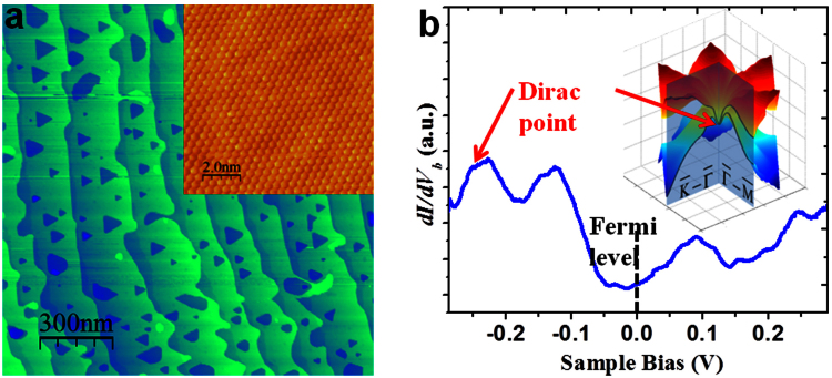
Based on an inverted bulk band order, antimony thin films presumably could become topological insulators if quantum confinement effect opens up a gap in the bulk bands. Coupling between topological surface states (TSS) from opposite surfaces, however, tends to degrade or even destroy their novel characters. Here the evolution and coupling of TSS on Sb(111) thin films from 30 bilayers down to 4 bilayers was investigated using in-situ Fourier-transform scanning tunneling spectroscopy and density functional theory computations. On a 30-bilayer sample, quasi-particle interference patterns are generated by the scattering of TSS from the top surface only. As the thickness decreases, inter-surface coupling degrades spin polarisation of TSS and opens up new wavevector-dependent scattering channels, resulting in spin degenerate states in most part of the surface Brillouin zone, whereas the TSS near the zone centre exhibit little inter-surface coupling, so they remain spin-polarised without opening a gap at the Dirac point.
Figures
 on Sb(111). By cutting the bands with vertical planes passing
  and
and  axes, the dispersions lines of SS along these high symmetry directions can be obtained.
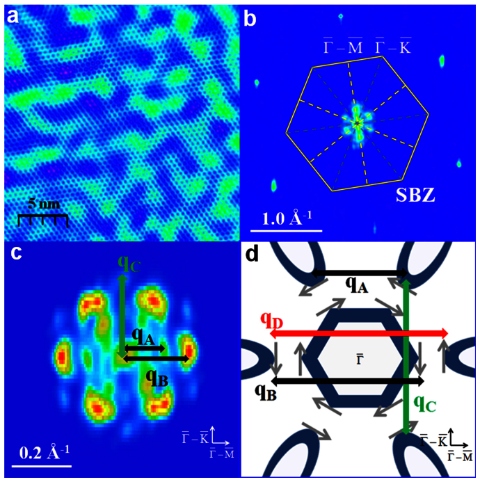
 . The first SBZ (yellow hexagon) and high symmetry directions are marked. (c) FT-STS pattern around
  with three observable scattering vectors qA, qBand qC. It was taken on a 40 nm × 40 nm area at Vb = 20 mV. (d) Schematic of CEC as well as the spin texture around
  , which has a central electron pocket and six hole pockets. The small grey arrows represent the spin directions. qAand qB are allowed scattering vectors, while qC is low in probability and qD totally forbidden.
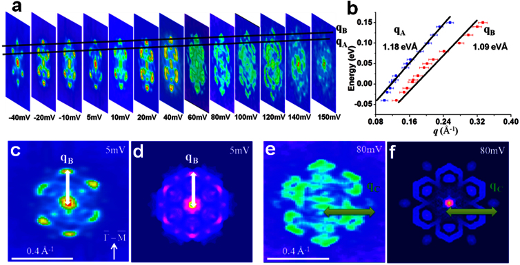
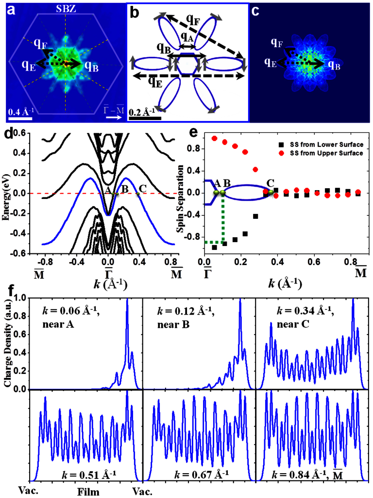
 . The blue lines represent the SS band chosen for computing the spin separation. (e) Spin separation as a function of k, indicating strong k-dependent inter-surface coupling of SS. A, B and C are the intersection points of CEC at EF with k axis along
  . (f) The real-space distributions of SS from near
  to
to  obtained from DFT computations, showing that a well-defined localization of SS around
  but large penetration depth for states from 0.34 Å−1 to
  .
.
Similar articles
-
Robust two-dimensional topological insulators in methyl-functionalized bismuth, antimony, and lead bilayer films.Nano Lett. 2015 Feb 11;15(2):1083-9. doi: 10.1021/nl504037u. Epub 2015 Jan 7. Nano Lett. 2015. PMID: 25559879
-
Electric-field tuning of the surface band structure of topological insulator Sb2Te3 thin films.Phys Rev Lett. 2013 Aug 2;111(5):056803. doi: 10.1103/PhysRevLett.111.056803. Epub 2013 Jul 30. Phys Rev Lett. 2013. PMID: 23952429
-
Annealing-Induced Bi Bilayer on Bi2Te3 Investigated via Quasi-Particle-Interference Mapping.ACS Nano. 2016 Sep 27;10(9):8778-87. doi: 10.1021/acsnano.6b04508. Epub 2016 Sep 7. ACS Nano. 2016. PMID: 27584869
-
Interfacial protection of topological surface states in ultrathin Sb films.Phys Rev Lett. 2012 Apr 27;108(17):176401. doi: 10.1103/PhysRevLett.108.176401. Epub 2012 Apr 25. Phys Rev Lett. 2012. PMID: 22680887
-
Quantum Anomalous Hall Effect in Magnetic Doped Topological Insulators and Ferromagnetic Spin-Gapless Semiconductors-A Perspective Review.Small. 2020 Oct;16(42):e1904322. doi: 10.1002/smll.201904322. Epub 2020 Sep 11. Small. 2020. PMID: 32914584 Review.
Cited by
-
Topological Surface-Dominated Spintronic THz Emission in Topologically Nontrivial Bi1- x Sbx Films.Adv Sci (Weinh). 2022 Jul;9(21):e2200948. doi: 10.1002/advs.202200948. Epub 2022 May 21. Adv Sci (Weinh). 2022. PMID: 35596613 Free PMC article.
-
Probing the Spin-Momentum Locking on Rashba Surfaces via Spin Current.ACS Appl Mater Interfaces. 2025 Mar 5;17(9):13162-13169. doi: 10.1021/acsami.4c06090. Epub 2024 Jul 16. ACS Appl Mater Interfaces. 2025. PMID: 39013007 Free PMC article. Review.
-
Studies on the origin of the interfacial superconductivity of Sb2Te3/Fe1+yTe heterostructures.Proc Natl Acad Sci U S A. 2020 Jan 7;117(1):221-227. doi: 10.1073/pnas.1914534117. Epub 2019 Dec 19. Proc Natl Acad Sci U S A. 2020. PMID: 31857387 Free PMC article.
-
Strain induced topological phase transitions in monolayer honeycomb structures of group-V binary compounds.Sci Rep. 2015 Dec 10;5:17980. doi: 10.1038/srep17980. Sci Rep. 2015. PMID: 26656257 Free PMC article.
-
Pressure-induced topological phase transition in noncentrosymmetric elemental tellurium.Proc Natl Acad Sci U S A. 2019 Dec 17;116(51):25530-25534. doi: 10.1073/pnas.1905524116. Epub 2019 Dec 4. Proc Natl Acad Sci U S A. 2019. PMID: 31801879 Free PMC article.
References
-
- Hsieh D. et al. Observation of unconventional quantum spin textures in topological insulators. Science 323, 919–922 (2009). - PubMed
-
- Chen Y. L. et al. Experimental Realization of a Three-Dimensional Topological Insulator, Bi2Te3. Science 325, 178–181 (2009). - PubMed
-
- Hsieh D. et al. A topological Dirac insulator in a quantum spin Hall phase. Nature 452, 970–974 (2008). - PubMed
-
- Hsieh D. et al. A tunable topological insulator in the spin helical Dirac transport regime. Nature 460, 1101–1105 (2009). - PubMed
-
- Roushan P. et al. Topological surface states protected from backscattering by chiral spin texture. Nature 460, 1106 (2009). - PubMed
LinkOut - more resources
Full Text Sources
Other Literature Sources
Research Materials
Miscellaneous
