

Reversible loss of Bernal stacking during the deformation of few-layer graphene in nanocomposites
- PMID: 23899378
- PMCID: PMC3789269
- DOI: 10.1021/nn402830f
Reversible loss of Bernal stacking during the deformation of few-layer graphene in nanocomposites
Abstract
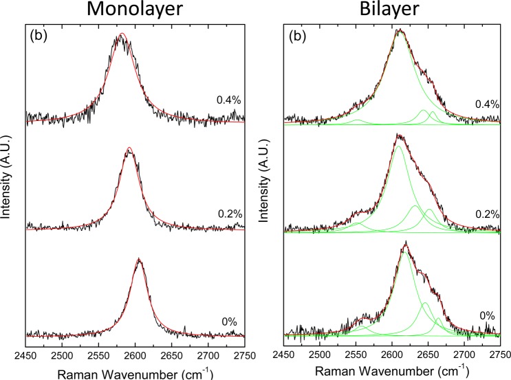
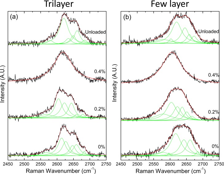
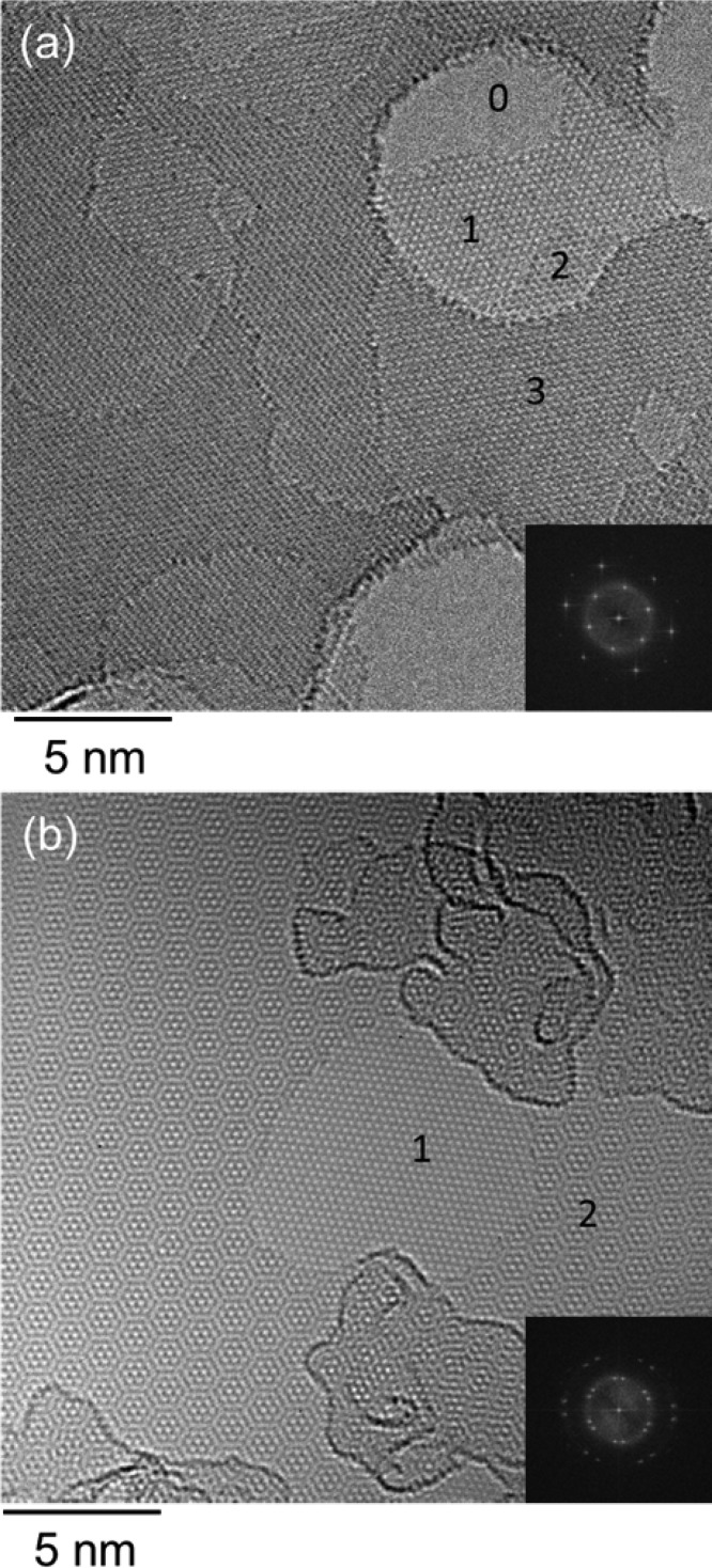
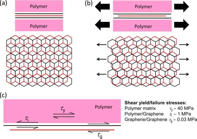
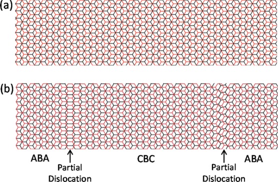
The deformation of nanocomposites containing graphene flakes with different numbers of layers has been investigated with the use of Raman spectroscopy. It has been found that there is a shift of the 2D band to lower wavenumber and that the rate of band shift per unit strain tends to decrease as the number of graphene layers increases. It has been demonstrated that band broadening takes place during tensile deformation for mono- and bilayer graphene but that band narrowing occurs when the number of graphene layers is more than two. It is also found that the characteristic asymmetric shape of the 2D Raman band for the graphene with three or more layers changes to a symmetrical shape above about 0.4% strain and that it reverts to an asymmetric shape on unloading. This change in Raman band shape and width has been interpreted as being due to a reversible loss of Bernal stacking in the few-layer graphene during deformation. It has been shown that the elastic strain energy released from the unloading of the inner graphene layers in the few-layer material (~0.2 meV/atom) is similar to the accepted value of the stacking fault energies of graphite and few layer graphene. It is further shown that this loss of Bernal stacking can be accommodated by the formation of arrays of partial dislocations and stacking faults on the basal plane. The effect of the reversible loss of Bernal stacking upon the electronic structure of few-layer graphene and the possibility of using it to modify the electronic structure of few-layer graphene are discussed.
Figures
References
-
- Geim A. K.; Novoselov K. S. The Rise of Graphene. Nat. Mater. 2007, 6, 183–191. - PubMed
-
- Novoselov K. S.; Geim A. K.; Morozov S. V.; Jiang D.; Zhang Y.; Dubonos S. V.; Grigorieva I. V.; Firsov A. A. Electric Field Effect in Atomically Thin Carbon Films. Science 2004, 306, 666–669. - PubMed
-
- Novoselov K. S.; Geim A. K.; Morozov S. V.; Jiang D.; Katsnelson M. I.; Grigorieva I. V.; Dubonos S. V.; Firsov A. A. Two-Dimensional Gas of Massless Dirac Fermions in Graphene. Nature 2005, 438, 197–200. - PubMed
-
- Lee C.; Wei X. D.; Kysar J. W.; Hone J. Measurement of the Elastic Properties and Intrinsic Strength of Monolayer Graphene. Science 2008, 321, 385–388. - PubMed
Publication types
LinkOut - more resources
Full Text Sources
Other Literature Sources
Molecular Biology Databases
