. 2013:3:2439.
doi: 10.1038/srep02439.

Exploring electronic structure of one-atom thick polycrystalline graphene films: a nano angle resolved photoemission study

Affiliations

Exploring electronic structure of one-atom thick polycrystalline graphene films: a nano angle resolved photoemission study

José Avila et al. Sci Rep. 2013.

Abstract

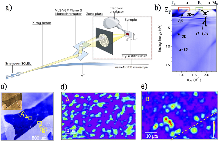
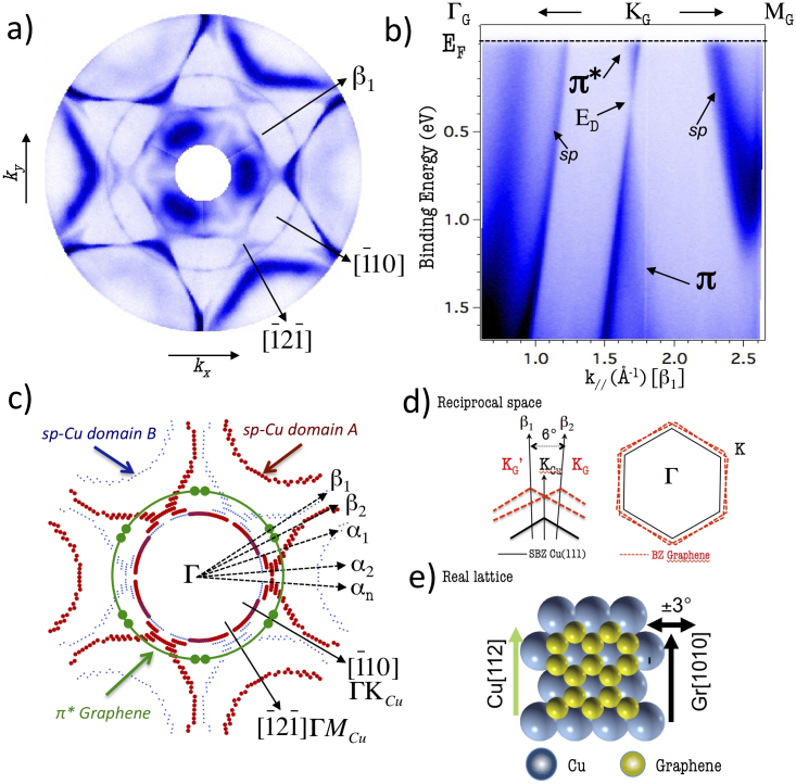
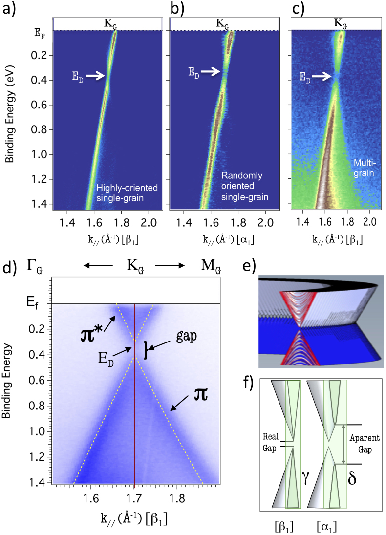
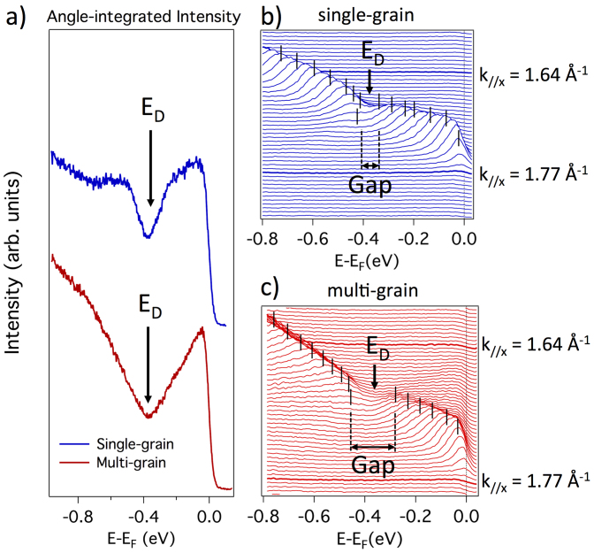
The ability to produce large, continuous and defect free films of graphene is presently a major challenge for multiple applications. Even though the scalability of graphene films is closely associated to a manifest polycrystalline character, only a few numbers of experiments have explored so far the electronic structure down to single graphene grains. Here we report a high resolution angle and lateral resolved photoelectron spectroscopy (nano-ARPES) study of one-atom thick graphene films on thin copper foils synthesized by chemical vapor deposition. Our results show the robustness of the Dirac relativistic-like electronic spectrum as a function of the size, shape and orientation of the single-crystal pristine grains in the graphene films investigated. Moreover, by mapping grain by grain the electronic dynamics of this unique Dirac system, we show that the single-grain gap-size is 80% smaller than the multi-grain gap recently reported by classical ARPES.


Figures

Figure 1
Figure 1. Mixed real- and reciprocal-space images of a polycrystalline graphene film, grown on copper foils.
(a) scheme of the nano-ARPES apparatus, connected to a beamline optics equipped with a focalization system composed by a pinhole, a Fresnel Zone plate and an Order Sorting Aperture (OSA). (b) micro-ARPES data inside one of a large copper grain of the sample. (c) real-space image of the copper states intensity (red box states of panel (b)) obtained by nano-ARPES mapping presented on a linear scale as a false-color image. The inset of panel (c) shows the optical image of the sample. Panels (d) and (e) show real-space images of graphene grains by monitoring the graphene states intensity (green box states of panel (b)) at the “A” and “B” yellow rectangles indicated in panel (c). Straight yellow dashed-line in panel (e) indicates the location of the corresponding Cu boundary grain.
Figure 2
Figure 2
(a) bottom line shows a typical XPS overview spectrum of graphene films grown by CVD on copper foils after air exposure for transfer purposes and a single 200°C one-hour annealing step. Top spectrum displays the same spectrum after the sample has been annealed up to 600°C, during 6 hours. (b) line-shape of C 1s photoelectron core level of the graphene film of panel (a), measured at the photon energy of 635 eV.(c) SEM image of graphene on a 50 μm thick copper foil. The image shows the presence of few graphene growth seeds (dark areas) together with dominant monolayer areas (light gray). (d) Raman spectra of a typical graphene film on copper foil. The small D peak (~ 1350 cm−1) and the intensity of the G' peak (~ 2700 cm−1) found to be more than twice as high as the G peak (~ 1580 cm−1) indicate the presence of high quality monolayer graphene.
Figure 3
Figure 3
(a) LEED pattern of a graphene film together with the six-fold single-crystal copper grain of the substrate. Panel (b) shows the real and reciprocal space of single- and multi- graphene grain. Moreover, the superposition of Dirac cones of graphene grains ramdomly oriented has been schematized.
Figure 4
Figure 4
Panel (a) shows the Fermi surface (FS) map of a graphene multi-grain film recorded at the B-box of figure 1c. Panel (b) displays the energy-momentum dispersion relations of π and π* bands near EF of graphene along the β direction, using linearly polarized light of 100 eV. A schematic diagram of the recorded FS is depicted in panel (c). Panel (e) depicts a sketch with the most favorable matching between the six-fold copper and graphene lattices.
Figure 5
Figure 5
Panel (a) and (b) show E-k dispersions measured by nano-ARPES in single pristine graphene grains oriented along the β and α directions, respectively, (see Fig. 4c). Panel (c) shows multi-grain E-k dispersion measured using micro-ARPES, along the β direction. Panel (d) displays the energy-momentum dispersion relations of π and π* bands near EF of multi-grain graphene film along the β direction, using circularly polarized light of 30 eV. Panel (f) depicts a schematic diagram representing the ARPES real and apparent gap at the Dirac point, depending on the γ- and δ- measurement plane, respectively.
Figure 6
Figure 6
Top and bottom curves of panel (a) show the angle-integrated photoemission spectrum of the single- and multi-grain, respectively, close to the Fermi level in a CVD graphene films grown on copper foil, along the β1 direction, taken with an angular aperture of 25 degree. Features at the Dirac point and the size of the bandgap can be easily discerned. Panels (b) and (c) display EDCs along ΓK direction (coincident with the β1 direction) in a single- and multi-grain graphene film, respectively. The n-doped gaphene bands disclose clearly the minimum intensity at the Dirac point and the difference between the actual and apparent gap size described in the text.

References

    1. Castro Neto A. H., Peres N. M. R., Novoselov K. S. & Geim A. K. The electronic properties of graphene. Rev. Mod. Phys. 81, 109–162 (2009).
    1. Avouris P., Chen Z. & Perebeinos V. Carbon-based electronics. Nat. Nanotechnol. 2, 605–615 (2007). - PubMed
    1. Novoselov K. S. et al. Two-dimensional gas of massless Dirac fermions in graphene. Nature 438, 197–200 (2005). - PubMed
    1. Meyer J. C. et al. The structure of suspended graphene sheets. Nature 446, 60–63 (2007). - PubMed
    1. Berger C. et al. Electronic confinement and coherence in patterned epitaxial graphene. Science 312, 1191–1196 (2006). - PubMed

Publication types

LinkOut - more resources