

Can we build a truly high performance computer which is flexible and transparent?
- PMID: 24018904
- PMCID: PMC3767948
- DOI: 10.1038/srep02609
Can we build a truly high performance computer which is flexible and transparent?
Abstract
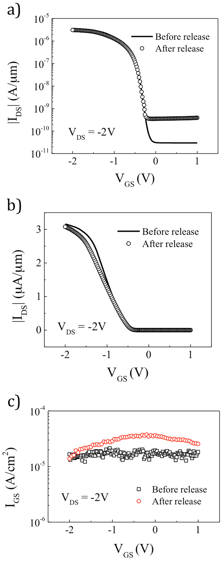
State-of-the art computers need high performance transistors, which consume ultra-low power resulting in longer battery lifetime. Billions of transistors are integrated neatly using matured silicon fabrication process to maintain the performance per cost advantage. In that context, low-cost mono-crystalline bulk silicon (100) based high performance transistors are considered as the heart of today's computers. One limitation is silicon's rigidity and brittleness. Here we show a generic batch process to convert high performance silicon electronics into flexible and semi-transparent one while retaining its performance, process compatibility, integration density and cost. We demonstrate high-k/metal gate stack based p-type metal oxide semiconductor field effect transistors on 4 inch silicon fabric released from bulk silicon (100) wafers with sub-threshold swing of 80 mV dec(-1) and on/off ratio of near 10(4) within 10% device uniformity with a minimum bending radius of 5 mm and an average transmittance of ~7% in the visible spectrum.
Figures


References
-
- Forrest S. R. The path to ubiquitous and low-cost organic electronic appliances on plastic. Nature 428, 911 (2004). - PubMed
-
- Reuss R. H. et al. Macroelectronics: Pers. Tech. and App. Proc. IEEE 93(7), 1239 (2005).
-
- Klauk H., Zschieschang U., Pflaum J. & Halik M. Ultralow-power organic complementary circuits. Nature 445, 745 (2007). - PubMed
-
- Xia Y., Kalihari V. & Frisbie C. D. Tetracene air-gap single-crystal field-effect transistors. Appl. Phys. Lett. 90, 162106 (2007).
-
- Kang S. J. et al. High-performance electronics using dense, perfectly aligned arrays of single-walled carbon nanotubes. Nature Nanotech. 2, 230 (2007). - PubMed
Publication types
LinkOut - more resources
Full Text Sources
Other Literature Sources
Research Materials
