

doi: 10.1021/nl401601x.
Epub 2013 Sep 27.
Introducing carbon diffusion barriers for uniform, high-quality graphene growth from solid sources
Affiliations
- PMID: 24024736
- PMCID: PMC3813970
- DOI: 10.1021/nl401601x
Item in Clipboard
Introducing carbon diffusion barriers for uniform, high-quality graphene growth from solid sources
Nano Lett.
.
Abstract
Carbon diffusion barriers are introduced as a general and simple method to prevent premature carbon dissolution and thereby to significantly improve graphene formation from the catalytic transformation of solid carbon sources. A thin Al2O3 barrier inserted into an amorphous-C/Ni bilayer stack is demonstrated to enable growth of uniform monolayer graphene at 600 °C with domain sizes exceeding 50 μm, and an average Raman D/G ratio of <0.07. A detailed growth rationale is established via in situ measurements, relevant to solid-state growth of a wide range of layered materials, as well as layer-by-layer control in these systems.
Figures
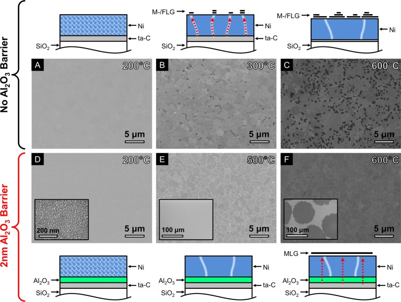
SEM micrographs
of Ni(550 nm)/ta-C(10 nm) (A–C) and Ni(550
nm)/Al2O3(2 nm)/ta-C(10 nm) (D–F) annealed
at 200 °C (A,D), 300 °C (B), 500 °C (E), 600 °C
(C,F) for 5 min (heated and cooled at a fixed rate of 100 °C
min–1). The inset of D shows a higher-magnification
micrograph of the sample showing the Ni grain structure (scale bar
is 200 nm). The insets of E,F show lower-magnification micrographs
of the same samples (scale bars are 100 μm). Sketches indicating
the effect of annealing for each of the samples are also shown.
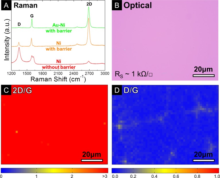
(A) Raman spectra of the M-/FLG grown from Ni(550 nm)/ta-C(10
nm)
(corresponding to Figure 1C), Ni(550 nm)/Al2O3(2 nm)/ta-C(10 nm) (corresponding to Figure 1F), and Au(5 nm)/Ni(550 nm)/Al2O3(2 nm)/ta-C(10 nm) samples annealed for 5 min at ∼600
°C and subsequently transferred to Si/SiO2(300 nm)
using the bubbling transfer method. (B) Optical micrograph of the
as-transferred MLG grown from a Au(5 nm)/Ni(550 nm)/Al2O3(2 nm)/ta-C(10 nm) sample under the annealing conditions
used in (A). The sheet resistance (RS)
of the as-transferred graphene is ∼1 kΩ/□, measured
using six contact Hall-geometry devices (see Methods). (C,D) Raman maps of 2D/G peak intensity (average 2D/G ratio of
∼3.5 with 100% of the area >2 ) (C) and D/G peak intensity
(average D/G ratio of <0.07) (D) for the region of graphene corresponding
to the optical micrograph in (B).
(A,B) In situ
XRR curves of a Ni(70 nm)/ta-C(10 nm)/SiO2(300 nm)/Si sample
taken during vacuum heating (base pressure ∼10–6 mbar) for reflecting angles (2θ) of 0.5–0.9°
(A) and 2–4.0° (B). The dashed horizontal arrow in A indicates
the shift in total reflective angle on heating, while the vertical
dashed lines in A and B indicate the oscillations associated with
the Ni and ta-C layers respectively. (C) In situ grazing incidence
XRD of a Ni(70 nm)/ta-C(10 nm)/SiO2(300 nm)/Si sample taken
during the same stepwise annealing process with a fixed incident angle
of αi = 0.75° (information depth of ∼80
nm). Note that the temperature-dependent shift in the reflection angles
is due to thermal expansion. A monochromatic X-ray beam of 11.5 keV
and a wavelength of 1.07812 Å (selected by a Si(111) double crystal
monochromator) is used, and the reflected/diffracted X-rays are measured
using a Mythen detector system. (D) Sketch showing the Ni/ta-C stacks
that were probed and indicating the diffusion of carbon to the exposed
catalyst surface which leads to M-/FLG formation.
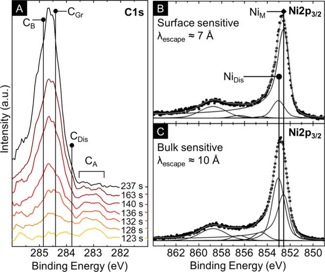
(A) Time-resolved in
situ XPS C1s core level lines for Ni(550 nm)/ta-C(10
nm) stacks during vacuum heating to ∼600 °C at ∼100
°C/min. Acquisition times are relative to the start of the heating
ramp from room temperature. Spectra are collected in normal emission
geometry at photon energies of 435 eV (surface sensitive; λescape ≈ 7 Å) with a spectral resolution of ∼0.3
eV. (B) Depth-resolved in situ XPS Ni2p3/2 core level lines
for Ni(550 nm)/ta-C(10 nm) stacks at the end of vacuum annealing at
∼600 °C. Spectra are background corrected (Shirley) and
collected in normal emission geometry at photon energies of 1010 eV
(surface sensitive; λescape ≈ 7 Å) and
1300 eV (bulk sensitive; λescape ≈ 10 Å)
with a spectral resolution of ∼0.3 eV. Increased information
depth is achieved using higher-incident X-ray energies and hence increased
electron mean free path lengths. The spectra are fitted using Doniach-Šùnjić
functions convoluted with Gaussian profiles with an accuracy of ∼0.05
eV. All binding energies are referenced to the Fermi edge.
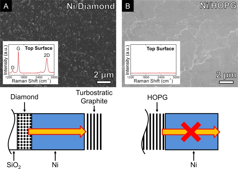
Scanning electron micrographs
of Ni(550 nm)/diamond(∼100
nm) (A) and Ni(550 nm)/HOPG (B) annealed at ∼600 °C for
5 min in vacuum (heated at a fixed rate of 100 °C min–1, cooled at ∼300 °C min–1). All scalebars
are 2 μm. Insets show the corresponding Raman spectra measured
on the as-grown samples. Sketches indicating the effect of annealing
on each of the samples are also shown.
References
-
- Novoselov K. S.; Fal’ko V. I.; Colombo L.; Gellert P. R.; Schwab M. G.; Kim K. Nature 2012, 490, 192–200. - PubMed
-
- Zheng M.; Takei K.; Hsia B.; Fang H.; Zhang X.; Ferralis N.; Ko H.; Chueh Y.-L.; Zhang Y.; Maboudian R.; Javey A. Appl. Phys. Lett. 2010, 96, 063110.
-
- Hofrichter J.; Szafranek B. N.; Otto M.; Echtermeyer T. J.; Baus M.; Majerus A.; Geringer V.; Ramsteiner M.; Kurz H. Nano Lett. 2010, 10, 36–42. - PubMed
-
- Suzuki S.; Takei Y.; Furukawa K.; Hibino H. Appl. Phys. Express 2011, 4, 065102.
-
- García J. M.; He R.; Jiang M. P.; Kim P.; Pfeiffer L. N.; Pinczuk A. Carbon 2011, 49, 1006–1012.
Publication types
MeSH terms
Substances
Grants and funding
LinkOut - more resources
Full Text Sources
Other Literature Sources
