. 2013 Oct 15;110(42):16748-53.
doi: 10.1073/pnas.1308885110. Epub 2013 Sep 30.

Graphene quantum point contact transistor for DNA sensing

Affiliations

Graphene quantum point contact transistor for DNA sensing

Anuj Girdhar et al. Proc Natl Acad Sci U S A. .

Abstract

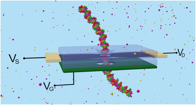
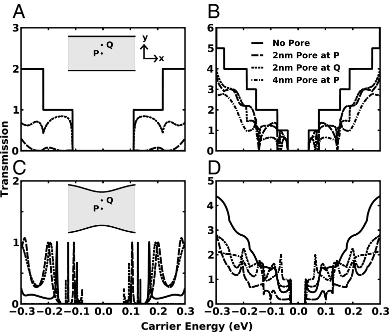
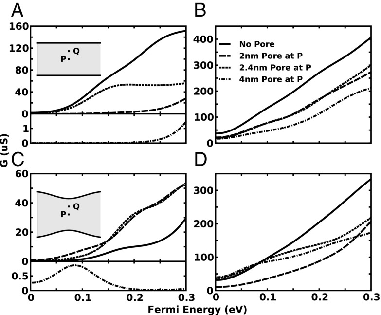
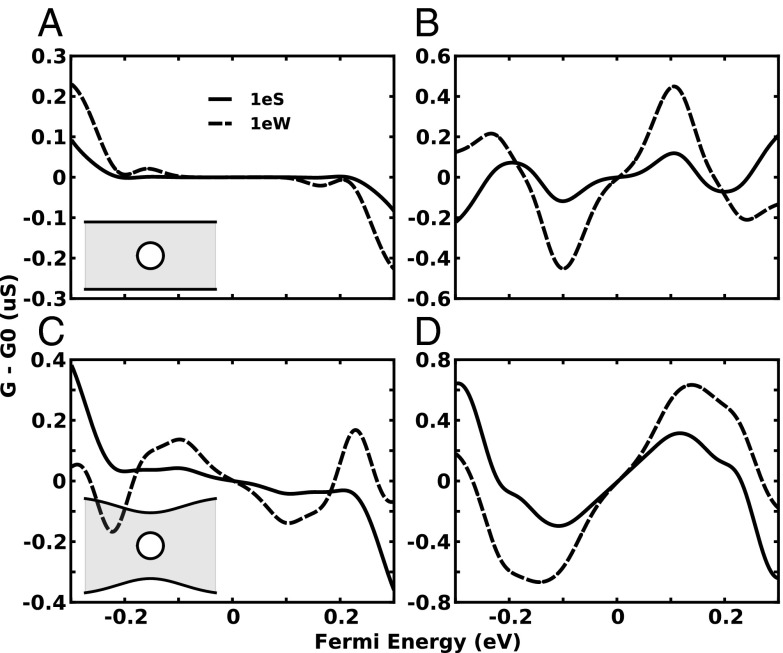
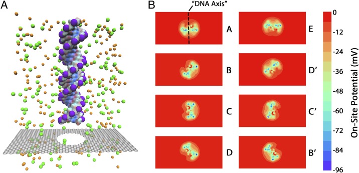
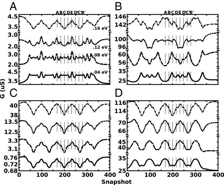
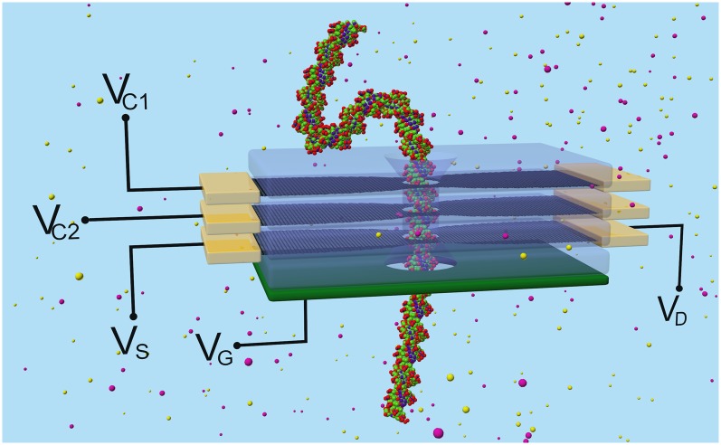
By using the nonequilibrium Green's function technique, we show that the shape of the edge, the carrier concentration, and the position and size of a nanopore in graphene nanoribbons can strongly affect its electronic conductance as well as its sensitivity to external charges. This technique, combined with a self-consistent Poisson-Boltzmann formalism to account for ion charge screening in solution, is able to detect the rotational and positional conformation of a DNA strand inside the nanopore. In particular, we show that a graphene membrane with quantum point contact geometry exhibits greater electrical sensitivity than a uniform armchair geometry provided that the carrier concentration is tuned to enhance charge detection. We propose a membrane design that contains an electrical gate in a configuration similar to a field-effect transistor for a graphene-based DNA sensing device.

Keywords: bio-molecule; simulation; solid-state membrane; transport.


Conflict of interest statement

The authors declare no conflict of interest.

Figures

Fig. 1.
Fig. 1.
Schematic diagram of a prototypical solid-state, multilayer device containing a GNR layer (black) with a nanopore, sandwiched between two oxides (transparent) atop a heavily doped Si back gate, VG (green). The DNA is translocated through the pore, and the current is measured with the source and drain leads, VS and VD (gold). (See SI Methods for a cross-sectional schematic diagram.)
Fig. 2.
Fig. 2.
Transmission functions for various edge geometries and pore configurations: (A) 5-nm (5-GNR)- and (B) 15-nm (15-GNR)-wide GNR-edged devices, (C) 8-nm (8-QPC)- and (D) 23-nm (23-QPC)-wide QPC-edged devices. Pristine (solid), a 2-nm pore at point P (long dash), a 2-nm pore at point Q (short dash), and a 4-nm pore at point P (dot–dash).
Fig. 3.
Fig. 3.
Conductance versus Fermi energy (as a function of carrier concentration) for the four edge geometries with four pore configurations for each geometry. (A) 5-GNR, (B) 15-GNR, (C) 8-QPC, and (D) 23-QPC. Pristine (solid), 2-nm pore at point P (long dash), 2-nm pore at point Q (short dash), and 4-nm pore at point P (dot–dash).
Fig. 4.
Fig. 4.
Change in the conductance due to adding an external charge within the 2-nm pore. “S” means the charge is placed 1/2 radius south of the center of the pore, and “W” means the charge is placed 1/2 radius west of the center of the pore. (A) 5-GNR, (B) 15-GNR, (C) 8-QPC, and (D) 23-QPC .
Fig. 5.
Fig. 5.
(A) Schematic of an AT DNA strand translocating through a pore. (B) Potential maps in the graphene plane due to the DNA molecule at eight successive snapshots throughout one full rotation of the DNA strand.
Fig. 6.
Fig. 6.
Conductance as a function of DNA position (snapshot) for multiple Fermi energies, 0.04 eV (solid), 0.08 eV (long dash), 0.12 eV (short dash), and 0.16 eV (dot–dash), as the DNA strand rigidly translocates through a 2.4-nm nanopore pore located at the device center (point P). (A) 5-GNR, (B) 15-GNR, (C) 8-QPC, and (D) 23-QPC.
Fig. 7.
Fig. 7.
Schematic diagram of a four-layer device containing two graphene layers (black) to control the translational motion of DNA through the nanopore. The top graphene layer (VC1) controls the translational speed of the DNA, whereas the second (VC2) controls the lateral confinement of the DNA within the nanopore. The third graphene layer (VDS) measures the sheet current. Finally, a heavily doped back gate (green) lies underneath the sheet current layer to control the carrier concentration. Oxide barriers (transparent) between different graphene layers provide electrical isolation. (See SI Methods for a cross-sectional schematic diagram).

References

    1. Branton D, et al. The potential and challenges of nanopore sequencing. Nat Biotechnol. 2008;26(10):1146–1153. - PMC - PubMed
    1. Schloss JA. How to get genomes at one ten-thousandth the cost. Nat Biotechnol. 2008;26(10):1113–1115. - PubMed
    1. Schadt EE, Turner S, Kasarskis A. A window into third-generation sequencing. Hum Mol Genet. 2010;19(R2):R227–R240. - PubMed
    1. Derrington IM, et al. Nanopore DNA sequencing with MspA. Proc Natl Acad Sci USA. 2010;107(37):16060–16065. - PMC - PubMed
    1. Li J, Gershow M, Stein D, Brandin E, Golovchenko JA. DNA molecules and configurations in a solid-state nanopore microscope. Nat Mater. 2003;2(9):611–615. - PubMed

Publication types