

Reversible insulator-metal transition of LaAlO₃/SrTiO₃ interface for nonvolatile memory
- PMID: 24100438
- PMCID: PMC3792417
- DOI: 10.1038/srep02870
Reversible insulator-metal transition of LaAlO₃/SrTiO₃ interface for nonvolatile memory
Abstract
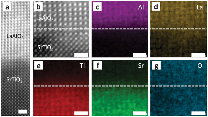
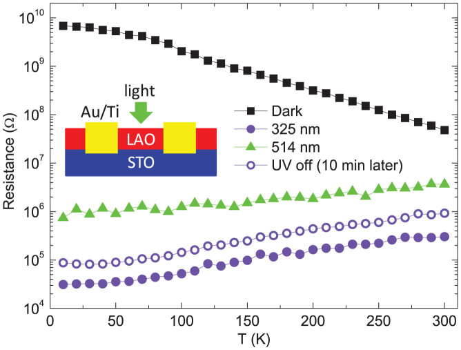
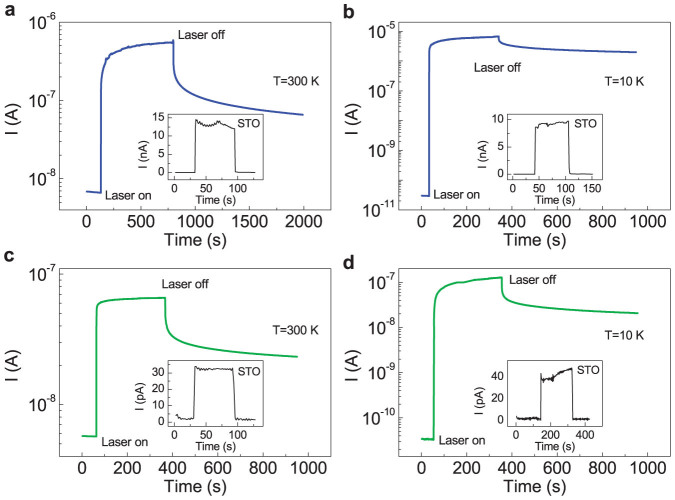
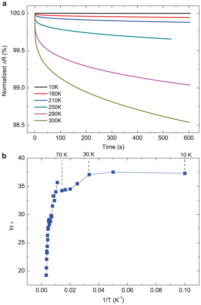
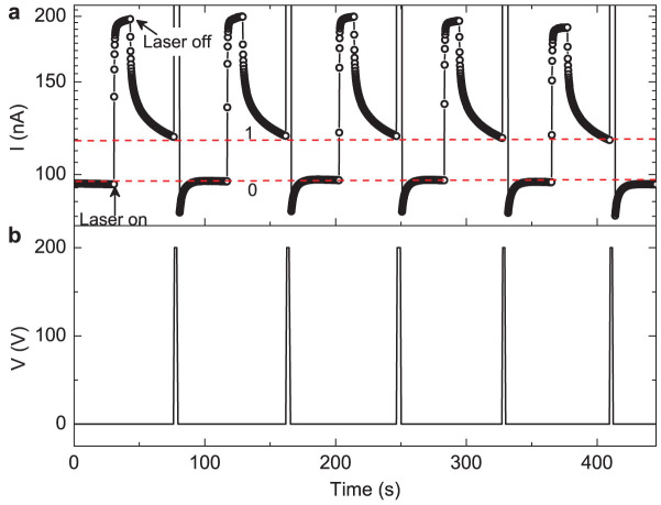
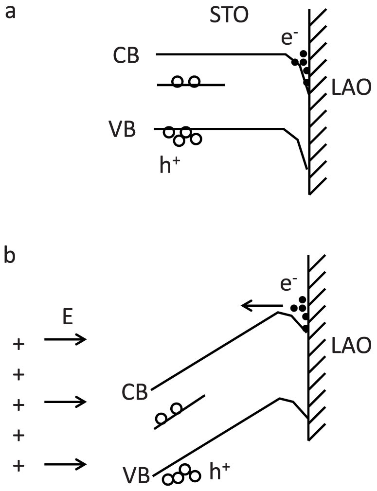
We report a new type of memory device based on insulating LaAlO₃/SrTiO₃ (LAO/STO) hetero-interface. The microstructures of the LAO/STO interface are characterized by Cs-corrected scanning transmission electron microscopy, which reveals the element intermixing at the interface. The inhomogeneous element distribution may result in carrier localization, which is responsible for the insulating state. The insulating state of such interface can be converted to metallic state by light illumination and the metallic state maintains after light off due to giant persistent photoconductivity (PPC) effect. The on/off ratio between the PPC and the initial dark conductance is as large as 10⁵. The metallic state also can be converted back to insulating state by applying gate voltage. Reversible and reproducible resistive switching makes LAO/STO interface promising as a nonvolatile memory. Our results deepen the understanding of PPC phenomenon in LAO/STO, and pave the way for the development of all-oxide electronics integrating information storage devices.
Figures
Similar articles
-
Room-temperature giant persistent photoconductivity in SrTiO₃/LaAlO₃ heterostructures.ACS Nano. 2012 Feb 28;6(2):1278-83. doi: 10.1021/nn203991q. Epub 2012 Jan 25. ACS Nano. 2012. PMID: 22260261
-
Anisotropic two-dimensional electron gas at the LaAlO₃/SrTiO₃ (110) interface.Nat Commun. 2013;4:1838. doi: 10.1038/ncomms2804. Nat Commun. 2013. PMID: 23673623 Free PMC article.
-
Creation of a two-dimensional electron gas at an oxide interface on silicon.Nat Commun. 2010 Oct 19;1:94. doi: 10.1038/ncomms1096. Nat Commun. 2010. PMID: 20981022
-
First-principles characterization of the critical thickness for forming metallic states in strained LaAlO₃/SrTiO₃(001) heterostructure.ACS Appl Mater Interfaces. 2014 Dec 24;6(24):22351-8. doi: 10.1021/am506336w. Epub 2014 Dec 8. ACS Appl Mater Interfaces. 2014. PMID: 25486683
-
Electronic and magnetic properties of SrTiO(3)/LaAlO(3) interfaces from first principles.Adv Mater. 2010 Jul 20;22(26-27):2881-99. doi: 10.1002/adma.200903800. Adv Mater. 2010. PMID: 20408133 Review.
Cited by
-
Photoresponse dynamics in amorphous-LaAlO3/SrTiO3 interfaces.Sci Rep. 2015 Feb 11;5:8393. doi: 10.1038/srep08393. Sci Rep. 2015. PMID: 25670163 Free PMC article.
-
Tuning of the magnetotransport properties of a spin-polarized 2D electron system using visible light.Sci Rep. 2023 Jun 21;13(1):10050. doi: 10.1038/s41598-023-36957-w. Sci Rep. 2023. PMID: 37344495 Free PMC article.
-
Anisotropic electrical resistance in mesoscopic LaAlO3/SrTiO3 devices with individual domain walls.Sci Rep. 2017 Mar 15;7:44361. doi: 10.1038/srep44361. Sci Rep. 2017. PMID: 28295058 Free PMC article.
-
Transition from a uni- to a bimodal interfacial charge distribution in [Formula: see text]/[Formula: see text] upon cooling.Sci Rep. 2020 Oct 27;10(1):18359. doi: 10.1038/s41598-020-74364-7. Sci Rep. 2020. PMID: 33110119 Free PMC article.
-
Enhanced surface-and-interface coupling in Pd-nanoparticle-coated LaAlO3/SrTiO3 heterostructures: strong gas- and photo-induced conductance modulation.Sci Rep. 2015 Feb 23;5:8531. doi: 10.1038/srep08531. Sci Rep. 2015. PMID: 25704566 Free PMC article.
References
-
- Ohtomo A. & Hwang H. Y. A High-mobility Electron Gas at the LaAlO3/SrTiO3 Heterointerface. Nature 427, 423–426 (2004). - PubMed
-
- Ben Shalom M., Ron A., Palevski A. & Dagan Y. Shubnikov-De Haas Oscillations in SrTiO3/LaAlO3 Interface. Phys. Rev. Lett. 105, 206401 (2010). - PubMed
-
- Caviglia A. D. et al. Two-Dimensional Quantum Oscillations of the Conductance at LaAlO3/SrTiO3 Interfaces. Phys. Rev. Lett. 105, 236802 (2010). - PubMed
-
- Thiel S., Hammerl G., Schmehl A., Schneider C. W. & Mannhart J. Tunable Quasi-Two-Dimensional Electron Gases in Oxide Heterostructures. Science 313, 1942–1945 (2006). - PubMed
-
- Bell C. et al. Dominant Mobility Modulation by the Electric Field Effect at the LaAlO3/SrTiO3 Interface. Phys. Rev. Lett. 103, 226802 (2009). - PubMed
Publication types
LinkOut - more resources
Full Text Sources
Other Literature Sources
