. 2014 Feb 21;43(4):1248-62.
doi: 10.1039/c3cs60258c.

Tip-enhanced near-field optical microscopy

Affiliations

Tip-enhanced near-field optical microscopy

Nina Mauser et al. Chem Soc Rev. .

Abstract

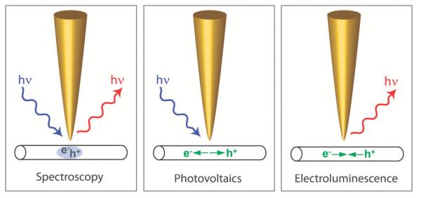
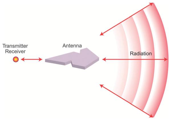
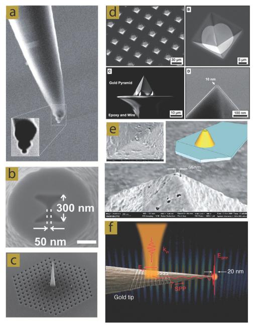
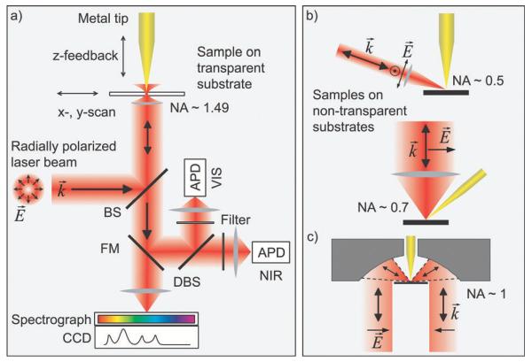
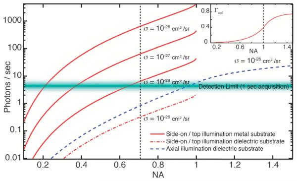
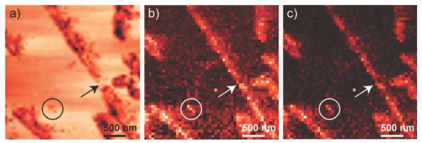
Tip-enhanced near-field optical microscopy (TENOM) is a scanning probe technique capable of providing a broad range of spectroscopic information on single objects and structured surfaces at nanometer spatial resolution and with highest detection sensitivity. In this review, we first illustrate the physical principle of TENOM that utilizes the antenna function of a sharp probe to efficiently couple light to excitations on nanometer length scales. We then discuss the antenna-induced enhancement of different optical sample responses including Raman scattering, fluorescence, generation of photocurrent and electroluminescence. Different experimental realizations are presented and several recent examples that demonstrate the capabilities of the technique are reviewed.


Figures

Fig. 1
Fig. 1
Optical antennas formed by metal nanostructures efficiently convert propagating radiation into localized energy in a nearby object. Conversely, localized energy is coupled to propagating radiation. Applications of antenna enhancement: (a) optical spectroscopy, (b) photovoltaics and (c) electroluminescence (adapted with permission from ref. . Copyright OSA 2009).
Fig. 2
Fig. 2
Transmitting/receiving antenna. Arrows indicate the direction of energy flow. The two configurations are related by the principle of reciprocity. In spectroscopy and microscopy, the two antenna concepts are combined; that is, the antenna is used both as a receiver and as a transmitter (Figure adapted with permission from ref. , ©2011 NPG.).
Fig. 3
Fig. 3
(a) Fluorescence from a single endohedral metallofullerene molecule as a function of separation between the molecule and the gold nanoparticle. At short separations the nanoparticle antenna enhances the fluorescence by a factor of ≈100. For a single nile blue molecule the enhancement is in the range of 8–10. Dots are experimental data and the solid line is a fit according to a dipole model (Reprinted with permission from J. Phys. Chem. C, 2010, 114, 7444. Copyright 2010 American Chemical Society.). (b) Influence of the intrinsic quantum yield of a fluorescence emitter q0 on the detected signal intensity for gold coated (blue solid circles), silicon (green open circles) and CNT (red open circles) tips. The signal is normalized to the signal detected for large tip-sample distances. The dashed line separates enhancement and quenching (Reprinted with permission from E. Shafran, B. D. Mangum and J. M. Gerton, Phys. Rev. Lett., 107, 037403 (2011). Copyright (2011) by the American Physical Society.).
Fig. 4
Fig. 4
Antenna-enhanced photocurrent microscopy. (a) Schematic of the experimental configuration using a carbon nanotube based device. (b) and (c) Simultaneously recorded zero-bias photocurrent and Raman scattering image, respectively. (d) Cross sections taken along the dashed lines in (b) and (c) together with fits using a Gaussian line shape function. The photocurrent signal features lower spatial resolution. The experimentally determined ratio of the Gaussian widths wPC/wR = 1.47 indicates that the photocurrent signal benefits only from excitation rate enhancement ∝f2 (Reprinted with permission from ACS Nano, 2012, 6, 6416. Copyright 2012 American Chemical Society.).
Fig. 5
Fig. 5
SEM images of different antenna structures. (a) Gold trimer antenna consisting of nanoparticles supported by a dielectric tip (Figure reproduced with permission from ref. , ©2011 NPG.). (b) Bowtie aperture antennas fabricated by FIB milling of an aluminum coated fiber probe (Reprinted with permission from Nano Lett., 2012, 12, 5972. Copyright 2012 American Chemical Society.). (c) Tapered plasmonic waveguide on top of a photonic crystal cavity for efficient photonic plasmonic coupling (Figure reproduced with permission from ref. , ©2010 NPG.). (d) Template-stripped 200 nm thick gold tips fabricated in anisotropically etched pyramidal molds on a Si wafer (Reprinted with permission from ACS Nano, 2012, 6, 9168. Copyright 2012 American Chemical Society.). (e) Coaxial antenna incorporated on the end of a scanning probe tip (Reprinted with permission from Nano Lett., 2011, 11, 1201. Copyright 2011 American Chemical Society.). (f) Etched gold wire tip with grating structure for SPP coupling and plasmonic nanofocusing (Reprinted with permission from J. Phys. Chem. Lett., 2012, 3, 945. Copyright 2012 American Chemical Society.).
Fig. 6
Fig. 6
(a) Schematic of an experimental setup employing on-axis illumination of a transparent sample used to observe simultaneous Raman scattering and photoluminescence of carbon nanotubes. A sharp metal tip is positioned in a tightly focused radially polarized laser beam. The optical signal is detected either by two avalanche photodiodes (APDs) for the VIS and NIR spectral range or by a combination of a spectrograph and a CCD. (b) Side-illumination of the tip on top of a non-transparent substrate. (c) Focusing of light using a parabolic mirror with high numerical aperture. To generate a strong field component parallel to the tip axis required for efficient field enhancement, scheme (a) and (c) utilize a radially polarized laser mode.-
Fig. 7
Fig. 7
Number of detected photons on a detector pixel as a function of the objective NA. Red curves are in a side-on/top illumination geometry with and without the use of a metallic substrate as indicated. With the dielectric substrate, we assume a Raman enhancement of ≈105. The dashed line indicates the maximum NA achievable in side-on illumination without the use of a parabolic mirror. The blue curve is under axial illumination (nsubstrate = noil = 1.5). The collection efficiency (inset) of the oil-immersion lens under axial illumination is based on results from ref. . The increased emission of light into the denser medium at angles greater than the critical angle is highly beneficial to TERS measurements. Thick green line represents the detection limit for 1 s acquisition time. It can be seen that side illumination benefits significantly from the increased field enhancement that arises due to plasmonic coupling to the metallic substrate. In contrast, the emission pattern of an emitter placed on a dielectric substrate significantly increases collection efficiency in an axial geometry when using oil-immersion objectives (Reprinted with permission from ref. . Copyright 2010 Elsevier.).
Fig. 8
Fig. 8
Simultaneously acquired (a) STM and (b and c) TERS (acquisition time 1 s per pixel, 2 mW incident power) images of individual nanotapes formed from beta-amyloid(1–40) peptide fragments (50 × 50 pixels). The color-coded TERS images display the intensity (high intensity is represented by a brighter pixel) of the aromatic ring breathing marker band (1004 cm −1). (b) Value of the peak integral, and (c) peak maximum. The arrow and circle illustrate that areas weakly observed as a feature in the STM image can be identified as nanotape/peptide structures using TERS imaging (Reprinted with permission from ACS Nano, 2013, 7, 911. Copyright 2013 American Chemical Society.).
Fig. 9
Fig. 9
Spatially resolved TERS for ferroelectric domain imaging. (a) Topography of a BaTiO3 nanorod. (b) The spectrally integrated TERS signal for ferroelectric domain imaging. (c) Lateral cross section along the dashed lines in a and b of the region of high TERS signal (blue) and corresponding topography (black) on the rod. (d) Domain assignment based on the Raman selection rules for the TERS geometry used (figure reproduced with permission from ref. , ©2009 NPG.).
Fig. 10
Fig. 10
(a) Simultaneously recorded topographic (upper panel) and near-field optical images (lower panel). Laser power: 170 μW. Tip-sample distance: 3 nm. (b) Line profile through the topographic image with its correlated optical intensity. Strongest emission dominated by PL from the DIP film is observed at terraces. Emission spectra show additional characteristic Raman bands of DIP and a broad PL background from the gold tip used in the experiment (Reprinted with permission from D. Zhang et al. Phys. Rev. Lett., 2010, 104, 056601. Copyright (2010) by the American Physical Society.).
Fig. 11
Fig. 11
Antenna-enhanced imaging of photocurrent fluctuations along a single SWCNT device. (a) Topography image. The drain and source electrodes appear at the top and at the bottom of the image. (b and c) Antenna-enhanced photocurrent and Raman G-band image. The dashed yellow line marks the position of the central particle. (d) The integrated photocurrent signal from panel d after a slope subtraction (blue symbols). The local minimum and kinks in the band energy profile seen in panels d and e coincide with the locations of particles seen as peaks in the topography data (black curve in panel e and marked in panel d by dashed vertical lines). (e) Schematic band diagram. The local minimum cannot be resolved with a diffraction limited laser spot due to spatial averaging of photocurrent signals with opposite signs. (f) High-resolution spectroscopic imaging of the central region of the device showing the topography, photocurrent, Raman D-band intensity and Raman G-band intensity. A varying defect induced D-band signal strength can be observed along the SWCNT, but without showing a correlation with the photocurrent signal (Reprinted with permission from ACS Nano, 2012, 6, 6416. Copyright 2012 American Chemical Society.).

References

    1. Novotny L. Progress in Optics. In: Wolf E, editor. Vol. 50. Elsevier; Amsterdam, The Netherlands: 2007. p. 137.
    1. Hartschuh A. Angew. Chem., Int. Ed. 2008;47:8178. - PubMed
    1. Yeo BS, Stadler J, Schmid T, Zenobi R, Zhang W. Chem. Phys. Lett. 2009;472:1.
    1. Ming T, Chen H, Jiang R, Li Q, Wang F. J. Phys. Chem. Lett. 2012;3:191.
    1. Pettinger B, Schambach P, Villagómez CJ, Scott N. Annu. Rev. Phys. Chem. 2012;63:379. - PubMed