. 2013 Dec;8(12):952-8.
doi: 10.1038/nnano.2013.219. Epub 2013 Oct 27.

Highly efficient gate-tunable photocurrent generation in vertical heterostructures of layered materials

Affiliations

Highly efficient gate-tunable photocurrent generation in vertical heterostructures of layered materials

Woo Jong Yu et al. Nat Nanotechnol. 2013 Dec.

Abstract

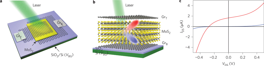
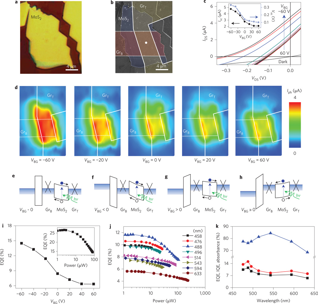
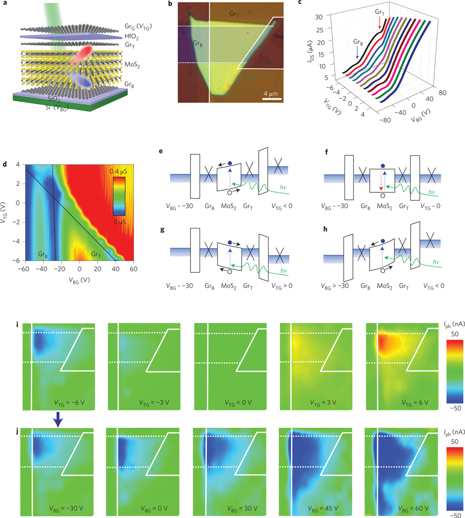
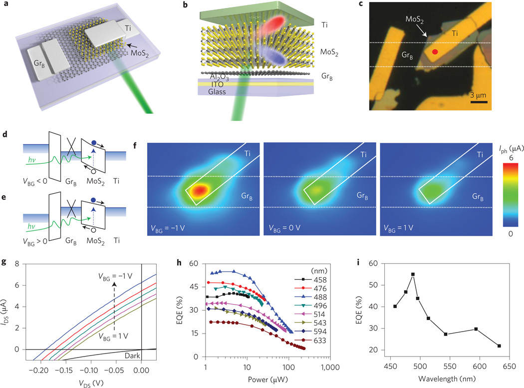
Layered materials of graphene and MoS₂, for example, have recently emerged as an exciting material system for future electronics and optoelectronics. Vertical integration of layered materials can enable the design of novel electronic and photonic devices. Here, we report highly efficient photocurrent generation from vertical heterostructures of layered materials. We show that vertically stacked graphene-MoS₂-graphene and graphene-MoS₂-metal junctions can be created with a broad junction area for efficient photon harvesting. The weak electrostatic screening effect of graphene allows the integration of single or dual gates under and/or above the vertical heterostructure to tune the band slope and photocurrent generation. We demonstrate that the amplitude and polarity of the photocurrent in the gated vertical heterostructures can be readily modulated by the electric field of an external gate to achieve a maximum external quantum efficiency of 55% and internal quantum efficiency up to 85%. Our study establishes a method to control photocarrier generation, separation and transport processes using an external electric field.


Figures

Figure 1
Figure 1. Photocurrent generation in vertical heterostructures of graphene–MoS2–graphene
a, Schematic illustration of the three-dimensional device layout. b, Schematic illustration of the side view of the device, with the semiconducting multilayer MoS2 sandwiched between the GrT and GrB electrodes. Red and blue colours indicate electrons and holes, respectively. The silicon substrate can be used as a back-gate electrode with 300 nm SiO2 as the dielectric layer. c, Experimental current–voltage characteristic of the vertical device in the dark (blue) and under illumination (red) by a focused laser beam (wavelength, 514 nm; power, 80 µW; spot size, 1 µm).
Figure 2
Figure 2. Field-effect modulated photocurrent generation in single-gated graphene–MoS2–graphene heterostructures
a, Optical image of the vertical heterostructure with a multilayer MoS2 flake (~50 nm thick) sandwiched between the GrT and GrB electrodes. b, SEM image of the same device with the GrT (yellow), GrB (red) and intermediate MoS2 layer (blue) labelled with different false colours. c, I–V characteristics of the device under laser illumination (on white dot in b) at VBG varying from −60 V to +60 V in steps of 20 V. Inset: variation of Isc and Voc with VBG. d, Scanning photocurrent images taken at gate biases between −60 V and +60 V under a 514 nm laser (excitation power, 80 µW; spot size, 1 µm). Dashed and solid lines indicate the edges of the GrB and GrT electrodes, respectively. e–h, Schematic band diagrams of the vertical heterostructure with zero (e), negative (f), positive (g) and large positive (h) bias on the silicon back gate. Blue dots, black circles and green arrows indicate electrons, holes and photons, respectively. i, EQE of the vertical heterostructure device as a function of back-gate voltage under 80 µW, 514 nm laser excitation. Inset: EQE of the device as a function of excitation laser power at VBG = −60 V. j, Excitation laser power-dependent EQE of another graphene-MoS2 (16 nm)-graphene device under various excitation wavelengths at VBG = −60 V. k, Wavelength-dependent EQE (black line with squares), absorbance (red line with circles) and IQE (blue line with triangles) of the device at VBG = −60 V under a focused laser power of 5 µW.
Figure 3
Figure 3. Field-effect switchable photocurrent generation in dual-gated graphene–MoS2–graphene heterostructures
a, Schematic illustration of the side view of the device, with a multilayer MoS2 flake sandwiched between the GrT and GrB electrodes, the silicon substrate as a back-gate electrode with a 300 nm SiO2 dielectric layer, and another graphene layer as the top-gate electrode (GrG) with a 60 nm HfO2 gate dielectric layer. b, Optical image of a dualgated device. c, Transfer characteristics of a dual-gated vertical heterostructure device as a function of VBG (−60 V to +60 V) at various VTG (−6 V to +4 V) at VDS = 100 mV. Blue and red arrows indicate the Dirac points of the GrB and GrT electrodes, respectively. d, Two-dimensional colour plot of the transconductance (dIDS/dVBG) of the dual-gated vertical heterostructure device. The Dirac points of the GrT and GrB electrodes are shown by solid and dashed lines, respectively. e–g, Schematic band diagrams of the dual-gated vertical heterostructure device with negative, zero and positive top-gate bias at a back-gate bias near the bottom graphene Dirac point (−30 V). The red dashed arrow in f indicates the recombination of electrons and holes. h, Schematic band diagram of the device with negative top-gate bias and more positive back-gate bias than the GrB Dirac point −30 V to further enhance the band slope and overall photocurrent. i, Scanning photocurrent images taken at VBG = −30 V and variable VTG (−6 V to +6 V) (under 80 µW, 514 nm laser excitation, with a spot size of 1 µm). Dashed and solid lines indicate the edges of the GrB and GrT electrodes, respectively. j, Scanning photocurrent images taken at fixed VTG = −6 V and variable VBG (−30 to +60 V).
Figure 4
Figure 4. Field-effect modulated photocurrent generation in a single-gated graphene–MoS2–metal heterostructure
a, Schematic three-dimensional illustration of the device layout. b, Schematic illustration of the side view of the device, with a multilayer MoS2 flake sandwiched between a GrB electrode and a top metal electrode (Ti). The device was fabricated on transparent ITO on a glass substrate (as the back gate) with 30-nm-thick Al2O3 as the gate dielectric to allow illumination to transmit through the back side of the substrate to reach the graphene–MoS2 contact. c, Optical image of a graphene–MoS2–metal heterostructure device. d,e, Schematic band diagrams of the graphene–MoS2–metal heterostructure at negative and positive back-gate voltages, respectively. f, Scanning photocurrent images taken at VBG = −1, 0 and +1 V (80µW, 514 nm excitation, with a spot size of 1 µm). Dashed and solid lines indicate the edges of the GrB and top metal electrodes, respectively. g, I–V characteristics of the device under laser illumination (on red dot in c) with VBG varying from −1 V to 1 V in steps of 0.5 V. The I–V curve obtained in the dark at VBG = −1 V passes through the origin, indicating that gate leakage is negligible. h, Excitation laser power-dependent EQE under various excitation wavelengths at VBG = −1 V. i, Wavelength-dependent EQE at a laser power of 5 µW.

References

    1. Novoselov KS, et al. A roadmap for grapheme. Nature. 2012;490:192–200. - PubMed
    1. Weiss NO, et al. Graphene: an emerging electronic material. Adv. Mater. 2012;24:5782–5825. - PMC - PubMed
    1. Schwierz F. Graphene transistors. Nature Nanotech. 2010;5:487–496. - PubMed
    1. Bonaccorso F, Sun Z, Hasan T, Ferrari AC. Graphene photonics and optoelectronics. Nature Photon. 2010;4:611–622.
    1. Avouris P. Graphene: electronic and photonic properties and devices. Nano Lett. 2010;10:4285–4294. - PubMed

Publication types