. 2013 Nov 26;7(11):10129-38.
doi: 10.1021/nn404331f. Epub 2013 Nov 13.

Continuous growth of hexagonal graphene and boron nitride in-plane heterostructures by atmospheric pressure chemical vapor deposition

Affiliations

Continuous growth of hexagonal graphene and boron nitride in-plane heterostructures by atmospheric pressure chemical vapor deposition

Gang Hee Han et al. ACS Nano. .

Abstract

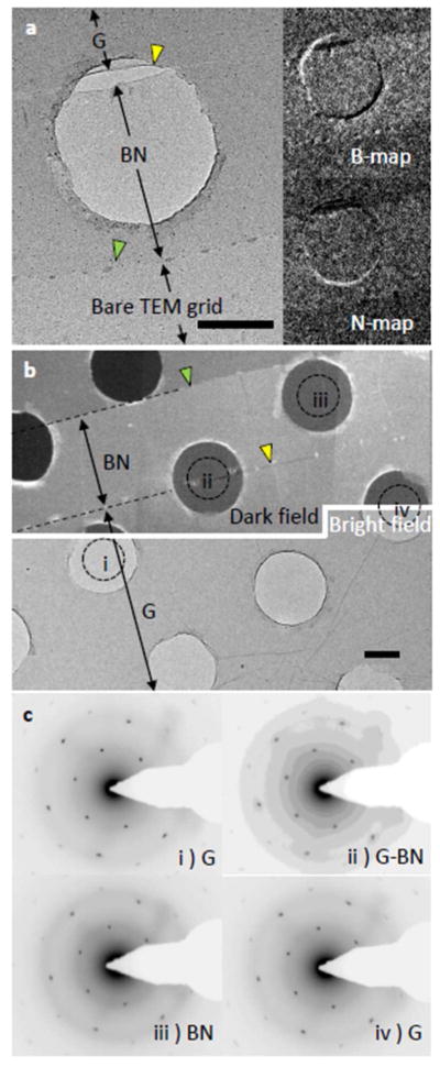
Graphene-boron nitride monolayer heterostructures contain adjacent electrically active and insulating regions in a continuous, single-atom thick layer. To date structures were grown at low pressure, resulting in irregular shapes and edge direction, so studies of the graphene-boron nitride interface were restricted to the microscopy of nanodomains. Here we report templated growth of single crystalline hexagonal boron nitride directly from the oriented edge of hexagonal graphene flakes by atmospheric pressure chemical vapor deposition, and physical property measurements that inform the design of in-plane hybrid electronics. Ribbons of boron nitride monolayer were grown from the edge of a graphene template and inherited its crystallographic orientation. The relative sharpness of the interface was tuned through control of growth conditions. Frequent tearing at the graphene-boron nitride interface was observed, so density functional theory was used to determine that the nitrogen-terminated interface was prone to instability during cool down. The electronic functionality of monolayer heterostructures was demonstrated through fabrication of field effect transistors with boron nitride as an in-plane gate dielectric.


Figures

Figure 1
Figure 1
Schematic and optical micrographs of continuous growth of graphene-boron nitride (G-BN) heterostructures. Graphene growth starts from seeds on the Cu foil (a) and hexagonal-BN grows continuously from the graphene template (left to right). b, c Low (b) and high (c) magnification image (of region marked with red solid rectangle in (b)) for G-BN heterostructure on the Cu growth substrate that was oxidized by hot plate baking (180 °C, 30 sec). In (c), the graphene flake and BN ribbon and flakes show differing optical contrast. (d) False color black, white and brown regions indicate graphene, BN, and bare Cu regions in (c), respectively. Scale bar in (b) is 50 μm, and the scale bar in (c) is 10 μm
Figure 2
Figure 2
Atomic force microscopy (AFM) analysis of G-BN heterostructures on Cu growth substrate and after transfer to a silicon dioxide surface (a–d) AFM images and line scans of G-BN heterostructure on Cu and (e–g) after transfer onto an oxidized silicon wafer. In (a–d), topographical AFM images were taken after baking at 180 °C for 1 min. Yellow and green triangles indicate the BN edge and G-BN boundary, respectively. (a) low-magnification image of G-BN flake (b) higher magnification topographic and (c) phase image from the dashed rectangle in Fig (a). (d) Height profiles of bare Cu-BN-G. (e) Topographical image of G-BN on SiO2 (300 nm oxide)/Si wafer, and (f) height profiles (1–3) in fig (e). (g) Phase-mode image shows the G-BN boundary clearly. Scale bar in (a), (e) and (g) is 4 μm. Scale bar in (b), (c) is 1 μm.
Figure 3
Figure 3
1D Raman maps of G-BN and BN structures (a) 1d Raman spectrum map across G-BN (top) and BN ribbons (BNR, bottom) after graphene removal by heat treatment (500 °C, 3 h) in air. (b) Raman spectrum of the BNR showing the characteristic peak of BN centered near 1373 cm−1. (c, d) Optical micrographs before (c) and after (d) the heat treatment used to remove graphene. Contrast and gamma values of (d) were modified to enhance the visibility of the BN nanoribbons on the substrate. Scale bars are 10 μm.
Figure 4
Figure 4
Transmission electron microscopy (TEM) and electron diffraction (ED) analysis. (a) TEM image of a region containing both a G-BN boundary (yellow arrow) and a BN ribbon with its termination (green arrow). Scale bar is 400 nm. Inset: Energy filtered images for B and N, proving that BN is present only in the ribbon region. (b) Composite dark-field (top)/bright-field (bottom)-TEM image and ED data confirming that the graphene and BN regions have the same crystallographic orientation (see text). (c) ED patterns were taken from the areas labeled as i, ii, iii and iv in Fig (b) (each diffraction pattern was taken from a 0.6 Lm diameter area).
Figure 5
Figure 5
DFT calculations of G-BN and related structures (a) Calculated dependence of tearing energy versus temperature with p(H2)=0.01 atm. Black, red, purple and light blue curves indicate tearing energies of BN, graphene, B-terminated G-BN and N-terminated G-BN, respectively. (b) Real-space charge density of G-BN. N-terminated G-BN (right) is predicted to be weaker than B-terminated G-BN (left) due to the presence of filled anti-bonding interfacial states.
Figure 6
Figure 6
Influence of ammonia borane (AB) pre-annealing time on G-BN growth a, b (a) 1-D Raman map from a G-BN sample grown using a 6 min pre-anneal of the AB source. (b) Raman spectra from the six locations indicated by white dashed lines in (a). c–e I-Vg measurements were taken from edge (blue dashed line, i, vii, viii) and middle (red dashed line, ii – vi) of the G-BN flake (c) I–Vg data from the selected area in Fig (d). (d) Optical image and 2-D Raman mapping (D/G) for the device. Solid boxes are the device channels. Scale bar, 4 μm. (e) Scanning electron micrograph of the device. The source (S) was fabricated as a common electrode. Scale bar, 20 μm.
Figure 7
Figure 7
Width control of boron nitride ribbon around graphene flake BN width around graphene controlled by growth time. (a) For 1–6 (top-bottom) min growth time, 6 min was used for pre-annealing. (b) Extracted growth rate is 57±4 nm/min. (C) Two graphene flakes (edges indicated by dashed black lines) are separated by a boron nitride gate dielectric region (edge shown by a solid yellow line). Scale bar is 10 um. (d) I–V characteristics for the device in (c).

References

    1. Novoselov KS, Geim AK, Morozov SV, Jiang D, Zhang Y, Dubonos SV, Grigorieva IV, Firsov AA. Electric Field Effect in Atomically Thin Carbon Films. Science. 2004;306:666–669. - PubMed
    1. Zhang Y, Tan YW, Stormer HL, Kim P. Experimental Observation of the Quantum Hall Effect and Berry’s Phase in Graphene. Nature. 2005;438:201– 204. - PubMed
    1. Bolotin KI, Sikes KJ, Jiang Z, Klima M, Fudenberg G, Hone J, Kim P, Stormer HL. Ultrahigh Electron Mobility in Suspended Graphene. Solid State Commun. 2008;146:351–355.
    1. Chen JH, Jang C, Xiao SD, Ishigami M, Fuhrer MS. Intrinsic and Extrinsic Performance Limits of Graphene Devices on Sio2. Nat Nanotechnol. 2008;3:206–209. - PubMed
    1. Britnell L, Gorbachev RV, Jalil R, Belle BD, Schedin F, Mishchenko A, Georgiou T, Katsnelson MI, Eaves L, Morozov SV, et al. Field-Effect Tunneling Transistor Based on Vertical Graphene Heterostructures. Science. 2012;335:947–950. - PubMed

Publication types

LinkOut - more resources