

High performance of graphene oxide-doped silicon oxide-based resistance random access memory
- PMID: 24261454
- PMCID: PMC3874615
- DOI: 10.1186/1556-276X-8-497
High performance of graphene oxide-doped silicon oxide-based resistance random access memory
Abstract
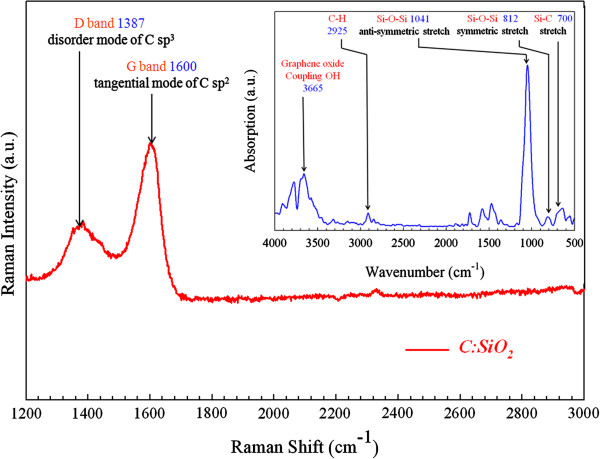
In this letter, a double active layer (Zr:SiOx/C:SiOx) resistive switching memory device with outstanding performance is presented. Through current fitting, hopping conduction mechanism is found in both high-resistance state (HRS) and low-resistance state (LRS) of double active layer RRAM devices. By analyzing Raman and FTIR spectra, we observed that graphene oxide exists in C:SiOx layer. Compared with single Zr:SiOx layer structure, Zr:SiOx/C:SiOx structure has superior performance, including low operating current, improved uniformity in both set and reset processes, and satisfactory endurance characteristics, all of which are attributed to the double-layer structure and the existence of graphene oxide flakes formed by the sputter process.
Figures


References
-
- Tsai CT, Chang TC, Chen SC, Lo I, Tsao SW, Hung MC, Chang JJ, Wu CY, Huang CY. Influence of positive bias stress on N2O plasma improved InGaZnO thin film transistor. Appl Phys Lett. 2010;8:242105. doi: 10.1063/1.3453870. - DOI
-
- Chen TC, Chang TC, Tsai CT, Hsieh TY, Chen SC, Lin CS, Hung MC, Tu CH, Chang JJ, Chen PL. Behaviors of InGaZnO thin film transistor under illuminated positive gate-bias stress. Appl Phys Lett. 2010;8:112104. doi: 10.1063/1.3481676. - DOI
-
- Yabuta H, Sano M, Abe K, Aiba T, Den T, Kumomi H. High-mobility thin-film transistor with amorphous InGaZnO4 channel fabricated by room temperature rf-magnetron sputtering. Appl Phys Lett. 2006;8:112123. doi: 10.1063/1.2353811. - DOI
-
- Chen TC, Chang TC, Hsieh TY, Lu WS, Jian FY, Tsai CT, Huang SY, Lin CS. Investigating the degradation behavior caused by charge trapping effect under DC and AC gate-bias stress for InGaZnO thin film transistor. Appl Phys Lett. 2011;8:022104. doi: 10.1063/1.3609873. - DOI
LinkOut - more resources
Full Text Sources
Other Literature Sources
