25th anniversary article: ordered polymer structures for the engineering of photons and phonons
- PMID: 24338738
- PMCID: PMC4227607
- DOI: 10.1002/adma.201303456
25th anniversary article: ordered polymer structures for the engineering of photons and phonons
Abstract
The engineering of optical and acoustic material functionalities via construction of ordered local and global architectures on various length scales commensurate with and well below the characteristic length scales of photons and phonons in the material is an indispensable and powerful means to develop novel materials. In the current mature status of photonics, polymers hold a pivotal role in various application areas such as light-emission, sensing, energy, and displays, with exclusive advantages despite their relatively low dielectric constants. Moreover, in the nascent field of phononics, polymers are expected to be a superior material platform due to the ability for readily fabricated complex polymer structures possessing a wide range of mechanical behaviors, complete phononic bandgaps, and resonant architectures. In this review, polymer-centric photonic and phononic crystals and metamaterials are highlighted, and basic concepts, fabrication techniques, selected functional polymers, applications, and emerging ideas are introduced.
Keywords: metamaterial; phononic crystal; photonic crystal; polymers.
© 2013 The Authors. Published by WILEY-VCH Verlag GmbH & Co. KGaA, Weinheim.
Figures


 with embedded air cylinders in a square lattice. The air cylinders have a radius
  , where
  is the lattice constant of the structure (inset). The partial PBG for TE-polarization is shown in red for the Γ−X and the Γ−M directions, respectively. (a2) The 2D photonic band diagram of the same structure with a higher permittivity of
  exhibiting a PBG for TM-polarized waves and for TE-polarized waves. However, since the TE and TM gaps do not overlap, there is no polarization-independent complete gap. (a3) The 2D photonic band diagram in (a2) is folded along the boundary of the irreducible BZ. (b) The phononic band diagram of the same structure with typical polymer solid density of
  = 1190 kg m−3, transverse sound speed
  = 1800 m/s, and longitudinal sound speed
  = 3100 m/s, respectively, for in-plane (solid lines) and out-of-plane (dashed lines) elastic waves.


 = 1.60) and low (
 = 1.45) indices and with the layer thickness equal to a quarter-wave optical thickness (
 ). Depending on the refractive index of the solvent (
 ) and the preference of the solvent for each type of polymer layer, a wide range of responses can occur.


 and
and  , respectively. The non-reciprocal behavior of the PT-symmetric system for the two different input beams (solid and dashed arrows) is illustrated.
 ) inside the PnBG propagates through a solid and is completely reflected by a solid/solid 2D PnC made of cylinders arranged in a triangular lattice embedded in a matrix. (a2) The sound wave of a frequency (
 ) outside the PnBG is transmitted through the PnC to the other side solid. Adapted from. (b1) An illustration of a 3D PnC consisting of lead spheres (
 ) arranged on a fcc lattice embedded in epoxy matrix. (b2) A phononic band diagram of the 3D PnC shows a large complete PnBG. Adapted with permission. (c) A mechanically switchable phononic device. The PnBG shifts due to the dramatic change in symmetry.
 = 0.53) is created from Bragg scattering of the impedance contrast
  of 6. (b1) Three-component PnC having an additional concentric very soft layer that serves to weakly couple the cylinders and the matrix and (b2) its band structure with displacement fields corresponding to the eigenmodes, C and D. A low frequency resonant PnBG (
 = 0.7) is created by using a soft shell (
 ) with impedance contrasts of
  of 50 and
  of 9. Adapted from. The color map for each mode indicates zero (blue) to a maximum displacement amplitude (red) with local directions and magnitudes of the displacements given by the arrows.

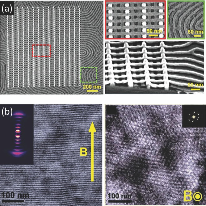
 direction, showing clear shifts in the peaks of modes 1 and 3, indicating a change in the propagation modes. The corresponding AFM images and Fourier transformed images (insets) indicate the breaking of the hexagonal symmetry due to the stretching. Reproduced with permission. Copyright 2006, American Chemical Society. (c) Tilted SEM image of AAO template without polymers (inset: top view). Experimental in-plane phononic dispersion relations of polyethylene glycol (PEG)- filled AAO (black symbols) and PDMS-filled AAO (red symbols) for the longitudinal acoustic branch 1 (open circles) and the weak flat branch 2 (open triangles). Reproduced with permission. Copyright 2010, American Chemical Society.
Similar articles
-
Micro-/nanostructured mechanical metamaterials.Adv Mater. 2012 Sep 18;24(36):4782-810. doi: 10.1002/adma.201201644. Epub 2012 Aug 17. Adv Mater. 2012. PMID: 22899377 Review.
-
Excitation and detection of acoustic phonons in nanoscale systems.Nanoscale. 2022 Sep 29;14(37):13428-13451. doi: 10.1039/d2nr04100f. Nanoscale. 2022. PMID: 36082529 Free PMC article. Review.
-
Optomechanical crystals.Nature. 2009 Nov 5;462(7269):78-82. doi: 10.1038/nature08524. Epub 2009 Oct 18. Nature. 2009. PMID: 19838165
-
Mechanical reinforcement of polymer colloidal crystals by supercritical fluids.J Colloid Interface Sci. 2020 Nov 1;579:786-793. doi: 10.1016/j.jcis.2020.06.104. Epub 2020 Jun 29. J Colloid Interface Sci. 2020. PMID: 32673855
-
Engineering thermal conductance using a two-dimensional phononic crystal.Nat Commun. 2014 Mar 19;5:3435. doi: 10.1038/ncomms4435. Nat Commun. 2014. PMID: 24647049 Free PMC article.
Cited by
-
Mechanically-Guided Deterministic Assembly of 3D Mesostructures Assisted by Residual Stresses.Small. 2017 Jun;13(24):10.1002/smll.201700151. doi: 10.1002/smll.201700151. Epub 2017 May 10. Small. 2017. PMID: 28489315 Free PMC article.
-
Lasing from dot-in-rod nanocrystals in planar polymer microcavities.RSC Adv. 2018 Apr 9;8(23):13026-13033. doi: 10.1039/c8ra01282b. eCollection 2018 Apr 3. RSC Adv. 2018. PMID: 35541227 Free PMC article.
-
Medial packing and elastic asymmetry stabilize the double-gyroid in block copolymers.Nat Commun. 2022 May 12;13(1):2629. doi: 10.1038/s41467-022-30343-2. Nat Commun. 2022. PMID: 35552400 Free PMC article.
-
Real-time and in situ observation of structural evolution of giant block copolymer thin film under solvent vapor annealing by atomic force microscopy.RSC Adv. 2019 Dec 23;10(1):70-75. doi: 10.1039/c9ra09043f. eCollection 2019 Dec 20. RSC Adv. 2019. PMID: 35492547 Free PMC article.
-
Ultrathin Photonic Polymer Gel Films Templated by Non-Close-Packed Monolayer Colloidal Crystals to Enhance Colorimetric Sensing.Polymers (Basel). 2019 Mar 21;11(3):534. doi: 10.3390/polym11030534. Polymers (Basel). 2019. PMID: 30960518 Free PMC article.
References
-
- Yablonovitch E. Phys. Rev. Lett. 1987;58:2059. - PubMed
-
- John S. Phys. Rev. Lett. 1987;58:2486. - PubMed
-
- Chen HY, Chan CT. Appl. Phys. Lett. 2007;91:183518.
-
- Cummer SA, Popa BI, Schurig D, Smith DR, Pendry J, Rahm M, Starr A. Phys. Rev. Lett. 2008;100:024301. - PubMed
-
- Zhang S, Xia CG, Fang N. Phys. Rev. Lett. 2011;106:024301. - PubMed
Publication types
MeSH terms
Substances
LinkOut - more resources
Full Text Sources
Other Literature Sources