

Surface passivation and optical characterization of Al2O3/a-SiCx stacks on c-Si substrates
- PMID: 24367740
- PMCID: PMC3869291
- DOI: 10.3762/bjnano.4.82
Surface passivation and optical characterization of Al2O3/a-SiCx stacks on c-Si substrates
Abstract
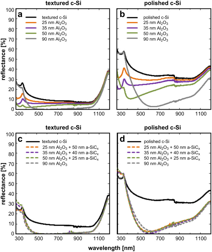
The aim of this work is to study the surface passivation of aluminum oxide/amorphous silicon carbide (Al2O3/a-SiCx) stacks on both p-type and n-type crystalline silicon (c-Si) substrates as well as the optical characterization of these stacks. Al2O3 films of different thicknesses were deposited by thermal atomic layer deposition (ALD) at 200 °C and were complemented with a layer of a-SiCx deposited by plasma-enhanced chemical vapor deposition (PECVD) to form anti-reflection coating (ARC) stacks with a total thickness of 75 nm. A comparative study has been carried out on polished and randomly textured wafers. We have experimentally determined the optimum thickness of the stack for photovoltaic applications by minimizing the reflection losses over a wide wavelength range (300-1200 nm) without compromising the outstanding passivation properties of the Al2O3 films. The upper limit of the surface recombination velocity (S eff,max) was evaluated at a carrier injection level corresponding to 1-sun illumination, which led to values below 10 cm/s. Reflectance values below 2% were measured on textured samples over the wavelength range of 450-1000 nm.
Keywords: aluminum oxide (Al2O3); antireflection coating; atomic layer deposition; silicon carbide (SiCx); surface passivation.
Figures


References
-
- Hofmann M, Janz S, Schmidt C, Kambor S, Suwito D, Kohn N, Rentsch J, Preu R, Glunz S W. Sol Energy Mater Sol Cells. 2009;93:1074–1078. doi: 10.1016/j.solmat.2008.11.056. - DOI
-
- Hoex B, Van de Sanden M C M, Schmidt J, Brendel R, Kessel W M M. Phys Status Solidi RRL. 2012;6:4–6. doi: 10.1002/pssr.201105445. - DOI
-
- Agostinelli G, Delabie A, Vitanov P, Alexieva Z, Dekkers H F W, De Wolfa S, Beaucarne G. Sol Energy Mater Sol Cells. 2006;90:3438–3442. doi: 10.1016/j.solmat.2006.04.014. - DOI
-
- Hoex B, Schmidt J, Bock R, Altermatt P P, van de Sanden M C M, Kessels W M M. Appl Phys Lett. 2007;91:112107. doi: 10.1063/1.2784168. - DOI
-
- Werner F, Veith B, Tiba V, Poodt P, Roozeboom F, Brendel R, Schmidt J. Appl Phys Lett. 2010;97:162103. doi: 10.1063/1.3505311. - DOI
LinkOut - more resources
Full Text Sources
Other Literature Sources