

25th anniversary article: organic field-effect transistors: the path beyond amorphous silicon
- PMID: 24443057
- PMCID: PMC4515091
- DOI: 10.1002/adma.201304346
25th anniversary article: organic field-effect transistors: the path beyond amorphous silicon
Abstract
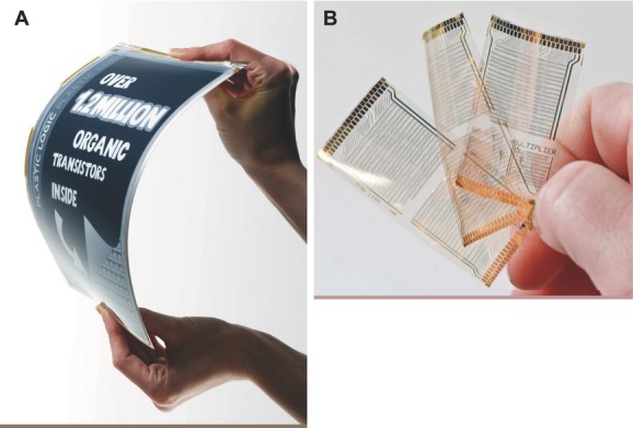
Over the past 25 years, organic field-effect transistors (OFETs) have witnessed impressive improvements in materials performance by 3-4 orders of magnitude, and many of the key materials discoveries have been published in Advanced Materials. This includes some of the most recent demonstrations of organic field-effect transistors with performance that clearly exceeds that of benchmark amorphous silicon-based devices. In this article, state-of-the-art in OFETs are reviewed in light of requirements for demanding future applications, in particular active-matrix addressing for flexible organic light-emitting diode (OLED) displays. An overview is provided over both small molecule and conjugated polymer materials for which field-effect mobilities exceeding > 1 cm(2) V(-1) s(-1) have been reported. Current understanding is also reviewed of their charge transport physics that allows reaching such unexpectedly high mobilities in these weakly van der Waals bonded and structurally comparatively disordered materials with a view towards understanding the potential for further improvement in performance in the future.
Keywords: organic field-effect transistors; organic light-emitting diode displays; organic semiconductors.
© 2014 The Authors. Published by WILEY-VCH Verlag GmbH & Co. KGaA, Weinheim.
Figures
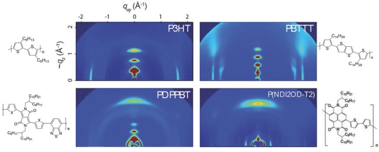
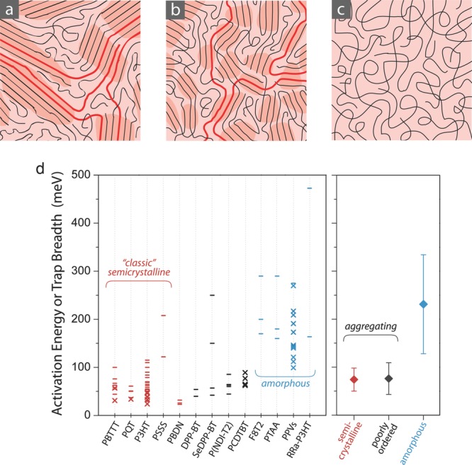
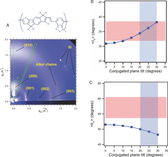
 ) as a function of the conjugated plane tilt, i.e., the angle between the (010) reflection and the conjugated plane normal for C16IDT-BT (B) and fast-dried, non-annealed P3HT (C). The upper and lower bounds of the pink areas in a denote the average orientation of the conjugated plane that is compatible with NEXAFS spectra (
 ) of top and buried interfaces, respectively. The light-blue areas highlight the conjugated plane tilt range between 20° and 30°: that is, the most probable conjugated plane tilt range for alkylated polythiophenes. For C16IDT-BT, the overlap between
  and the range of possible
 suggests that the conjugated planes are oriented in similar ways irrespective of whether their environments are crystalline or non-crystalline, whereas for P3HT the absence of overlap between the
  and
and  suggests that the orientation of the chains in non-crystalline environments is likely to be different from those in crystalline domains. Reproduced with permission.[81] Copyright 2013, Macmillan Publishers Ltd
References
-
- Davis EA, Mott NF. Philos. Mag. 1970;22:903.
-
- Coropceanu V, Cornil J, da Silva DA, Olivier Y, Silbey R, Bredas JL. Chem. Rev. 2007;107:2165. - PubMed
-
- Matsui H, Mishchenko AS, Hasegawa T. Phys. Rev. Lett. 2010;104:056602. - PubMed
-
- Troisi A. Chem. Soc. Rev. 2011;40:2347. - PubMed
-
- Sirringhaus H, Sakanoue T, Chang J-F. Phys. Status Solidi B. 2012;249:1655.
Publication types
LinkOut - more resources
Full Text Sources
Other Literature Sources
Miscellaneous
