. 2011 Nov 3;21(1):132-144.
doi: 10.1109/JMEMS.2011.2171326.

Novel First-Level Interconnect Techniques for Flip Chip on MEMS Devices

Affiliations

Novel First-Level Interconnect Techniques for Flip Chip on MEMS Devices

Jemmy Sutanto et al. J Microelectromech Syst. .

Abstract

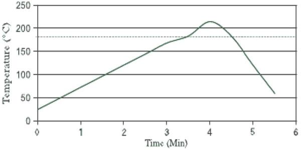
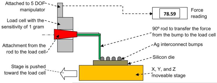
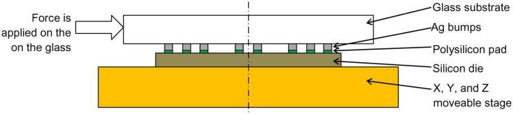
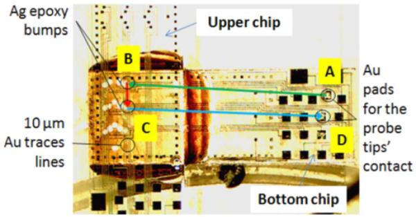
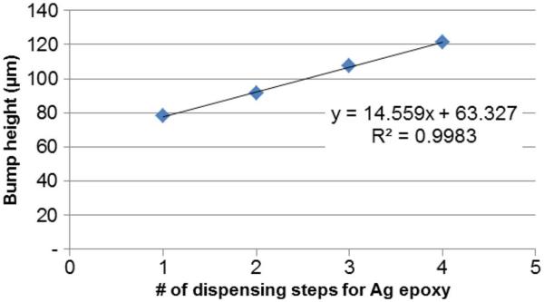
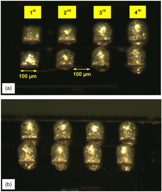
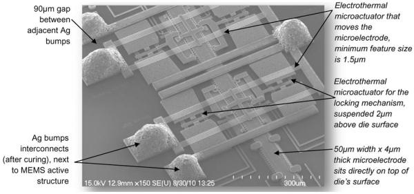
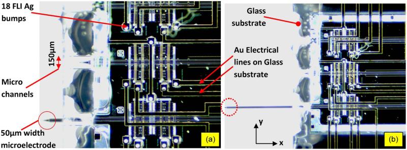
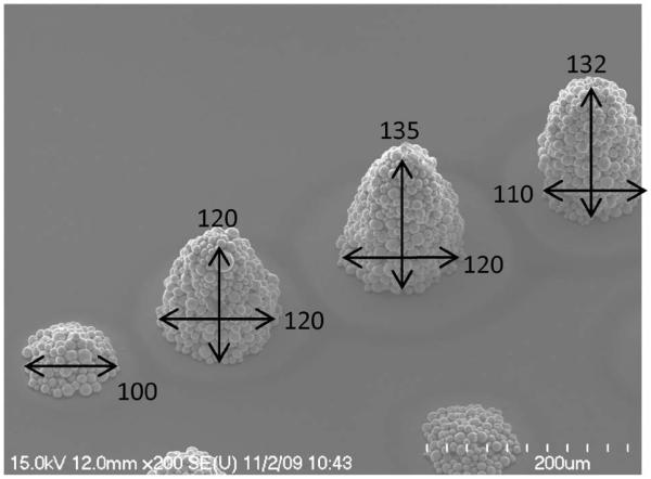
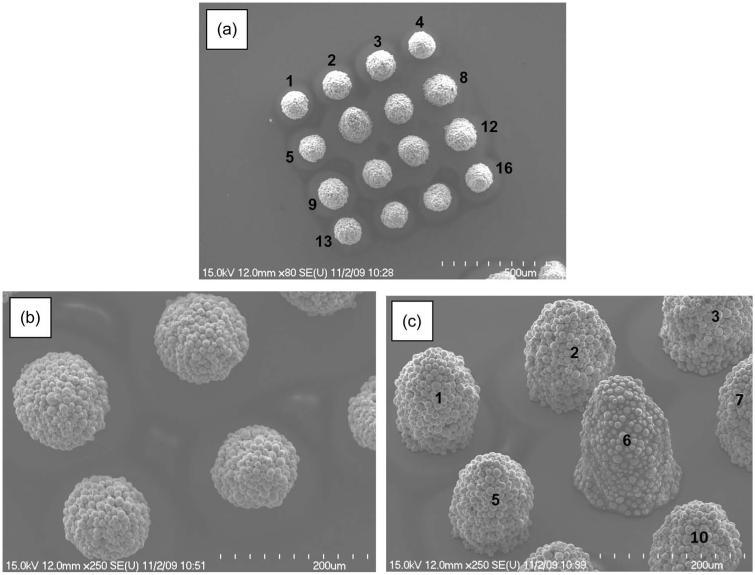
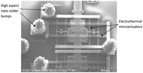
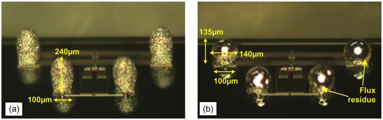
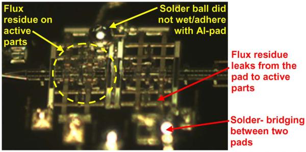
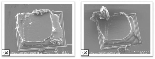
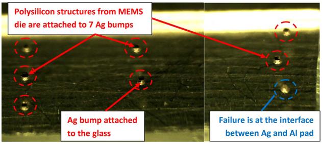
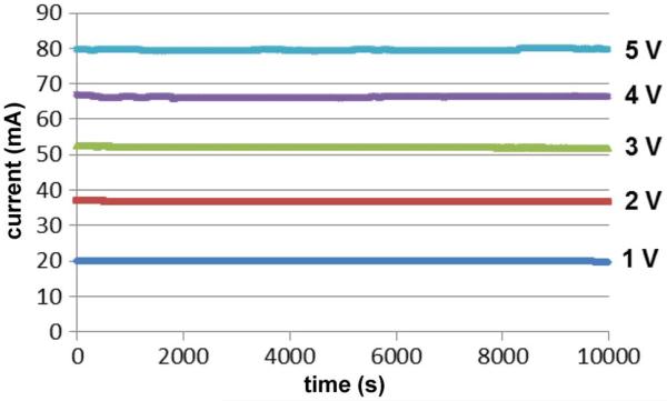
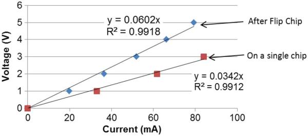
Flip-chip packaging is desirable for microelectro-mechanical systems (MEMS) devices because it reduces the overall package size and allows scaling up the number of MEMS chips through 3-D stacks. In this report, we demonstrate three novel techniques to create first-level interconnect (FLI) on MEMS: 1) Dip and attach technology for Ag epoxy; 2) Dispense technology for solder paste; 3) Dispense, pull, and attach technology (DPAT) for solder paste. The above techniques required no additional microfabrication steps, produced no visible surface contamination on the MEMS active structures, and generated high-aspect-ratio interconnects. The developed FLIs were successfully tested on MEMS moveable microelectrodes microfabricated by SUMMiTVTM process producing no apparent detrimental effect due to outgassing. The bumping processes were successfully applied on Al-deposited bond pads of 100 μm × 100 μm with an average bump height of 101.3 μm for Ag and 184.8 μm for solder (63Sn, 37Pb). DPAT for solder paste produced bumps with the aspect ratio of 1.8 or more. The average shear strengths of Ag and solder bumps were 78 MPa and 689 kPa, respectively. The electrical test on Ag bumps at 794 A/cm2 demonstrated reliable electrical interconnects with negligible resistance. These scalable FLI technologies are potentially useful for MEMS flip-chip packaging and 3-D stacking.

Keywords: 3-D stacks; BioMEMS; flip chip; flux contamination; interconnects; microchip; packaging; solder.


Figures

Fig. 1
Fig. 1
Illustration of the custom-made setup for flip-chip interconnect.
Fig. 2
Fig. 2
Schematic of the steps involved in the development of Ag bump interconnects through Dip and Attach technique (DAT).
Fig. 3
Fig. 3
Schematic of the steps involved in the development of solder bump interconnects through “dispense technique (DT).”
Fig. 4
Fig. 4
Schematic of the steps involved in the development of solder bump interconnects through “dispense, pull, and attach technique (DPAT)”.
Fig. 5
Fig. 5
Normal solder reflow process, adapted from Indium Inc. for 63Sn 37Pb solder paste.
Fig. 6
Fig. 6
Temperature profile during the optimal slow reflow process for creating solder bumps.
Fig. 7
Fig. 7
Schematic of the setup for shear stress characterization of Ag interconnect bumps.
Fig. 8
Fig. 8
Schematic of the setup for mechanical strength test of the Ag interconnect bumps after the flip-chip assembly on a glass substrate.
Fig. 9
Fig. 9
Flip-chip configuration for electrical test of the Ag interconnect bumps.
Fig. 10
Fig. 10
Bump height versus the number of Ag epoxy dispensing steps.
Fig. 11
Fig. 11
Micrographs (a) Ag epoxy bumps of increasing heights after successive dispensing steps and (b) showing the Ag epoxy bumps after four dispensing steps.
Fig. 12
Fig. 12
MEMS actuator with Ag bumps interconnects.
Fig. 13
Fig. 13
Fully packaged MEMS die (2.8 mm × 3.6 mm) flip chipped on a glass substrate. Ag bumps were used as the FLIs. (a): the bottom MEMS microelectrode, prior to actuation; (b): Bottom MEMS microelectrode after 2-mm actuation.
Fig. 14
Fig. 14
SEM image of solder bumps made using “dispense technique” (DT).
Fig. 15
Fig. 15
(a)–(c). SEM images of solder bumps made by “dispense, pull, and attach technique” (DPAT).
Fig. 16
Fig. 16
MEMS actuator with DPAT solder bumps interconnects, aspect ratio of 1.85 average.
Fig. 17
Fig. 17
(a) Four bumps are formed on Al pad by using DPAT process; the average height is approximately 240 μm—before the reflow process. (b) The four bumps after the standard reflow process, the average height is 135 μm; the flux residue is solidified at the base of the bumps. Bump shape is almost spherical.
Fig. 18
Fig. 18
Flux residue from the normal reflow process freezes the MEMS active part; the flux leaks from the perimeter of the pad to the active part during reflow process. This contamination is uncontrollable and causes the yield of bumping process to be significantly reduced.
Fig. 19
Fig. 19
Shear strength measurements on 15 bumps each of 63Sn37Pb and Ag.
Fig. 20
Fig. 20
(a) and (b). SEM of two typical Ag bump interconnects after the shear stress characterization.
Fig. 21
Fig. 21
Glass with eight Ag epoxy bump interconnects after shear stress test. Prior to the shear test, it was flip chipped on silicon chips with aluminum bond pads. The seven bumps shown in broken circles showed failure at the polysilicon pad–silicon die interface.
Fig. 22
Fig. 22
Measured current over time at different voltages for Ag bumps after flip chip.
Fig. 23
Fig. 23
Applied voltage versus measured current for electrical test on the Ag interconnect bumps (a) after flip chip and (b) on a single chip.

References

    1. Witvrouw A. CMOS-MEMS integration: Why, how and what?; Proc. ICCAD IEEE/ACM; San Jose, CA. 2006. pp. 826–827.
    1. Chen LT, Cheng WH. A novel plastic package for pressure sensors fabricated using the lithographic dam-ring approach. Sens. Actuators A, Phys. 2009 Jan.149:165–171.
    1. Pai RS, Walsh KM. The viability of anisotropic conductive film as a flip chip interconnect technology for MEMS devices. J. Micromech. Microeng. 2005 Jun.15(6):1131–1139.
    1. Candler RN, Park WT, Li HM, Partridge G. Yama, A., Lutz M, Kenny TW. Single wafer encapsulation of MEMS devices. IEEE Trans. Adv. Packag. 2003 Aug.26(3):227–232.
    1. Ayanoor-Vitikkate V, Chen KL, Park WT, Kenny TW. Development of wafer scale encapsulation process for large displacement piezoresistive MEMS devices. Sens. Actuators A, Phys. 2009 Dec.156(2):275–283.

LinkOut - more resources