. 2014 Feb 12:4:4077.
doi: 10.1038/srep04077.

High-Q CMOS-integrated photonic crystal microcavity devices

Affiliations

High-Q CMOS-integrated photonic crystal microcavity devices

Karan K Mehta et al. Sci Rep. .

Abstract

Integrated optical resonators are necessary or beneficial in realizations of various functions in scaled photonic platforms, including filtering, modulation, and detection in classical communication systems, optical sensing, as well as addressing and control of solid state emitters for quantum technologies. Although photonic crystal (PhC) microresonators can be advantageous to the more commonly used microring devices due to the former's low mode volumes, fabrication of PhC cavities has typically relied on electron-beam lithography, which precludes integration with large-scale and reproducible CMOS fabrication. Here, we demonstrate wavelength-scale polycrystalline silicon (pSi) PhC microresonators with Qs up to 60,000 fabricated within a bulk CMOS process. Quasi-1D resonators in lateral p-i-n structures allow for resonant defect-state photodetection in all-silicon devices, exhibiting voltage-dependent quantum efficiencies in the range of a few 10 s of %, few-GHz bandwidths, and low dark currents, in devices with loaded Qs in the range of 4,300-9,300; one device, for example, exhibited a loaded Q of 4,300, 25% quantum efficiency (corresponding to a responsivity of 0.31 A/W), 3 GHz bandwidth, and 30 nA dark current at a reverse bias of 30 V. This work demonstrates the possibility for practical integration of PhC microresonators with active electro-optic capability into large-scale silicon photonic systems.


Figures

Figure 1
Figure 1
(a) Photograph of full wafer, on which a single reticle (inset) was repeated. The location of the PhC devices discussed here is labeled within the inset. (b) Schematic chip cross-section (not to scale), illustrating (from left to right) doping profiles around nmos and pmos transistors with metal vias and copper wiring, intrinsic pSi waveguide structures separated from the silicon substrate by a 1.2 μm-thick Deep Trench Isolation (DTI) deposited oxide, and a doped and contacted electro-optic structure. (c) Detailed schematic including dimensions near optical cores. (d) Transformation of supplied (desired) pattern to mask design after optical proximity correction, and SEM images of 2D lattice of fabricated holes in pSi.
Figure 2
Figure 2
(a) Optical micrograph of a single cavity device, with grating couplers and tapers for input/output light coupling. (b) SEM image of pSi in a fabricated PhC device, with FDTD-calculated mode profile overlaid. (c) and (d) Measured transmission spectra through cavities with resonant wavelengths λ0 ≈ 1512 (a = 320 nm, w = 450 nm) and λ0 ≈ 1549 nm (a = 330 nm, w = 470 nm), respectively. Curves and fits for cavities with 8, 12 and 18 pairs of mirror holes are shown for each (black, red and blue curves), with (e) peak resonant transmissions fit to theoretical predictions as function of total quality factor, allowing extraction of intrinsic Qs of 58,000 (black curve for λ0 = 1512 nm cavity) and 51,000 (red curve, λ0 = 1549 nm).
Figure 3
Figure 3
(a) SEM image of detector structure with one optical input, with p+ and n+ implanted regions shaded. Measurements are presented in this figure for a device with intrinsic region width wi = 1.6 μm, as labeled. (b) IV characteristics without illumination and with 3 μW in-waveguide power at cavity resonance wavelength. (c) Photocurrent spectra at reverse bias of 22 V for powers logarithmically spaced between 1.6 and 120 μW input optical power, and (d) Peak QE vs. voltage and power for resonant pSi PhC defect-state photodetector.
Figure 4
Figure 4
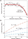
(a) Modulation response of detector with 1 μm intrinsic region, under 30 V reverse bias with an empirical fit showing 2.9 GHz 3-dB frequency. DC quantum efficiency at this operating point was 25% (responsivity 0.31 A/W), with a dark current of 30 nA. (b) Fit 3-dB frequencies for 3 different devices with identical optical design, but different intrinsic region widths (wi, as labeled; the middle curve shows results from the same device as in Fig. 3) as a function of applied reverse voltage. Lines are guides to the eye.

References

    1. Vahala K. J. Optical microcavities. Nature 424, 839–846 (2003). - PubMed
    1. Little B. E., Chu S. T., Haus H. A., Foresi J. & Laine J.-P. Microring resonator channel dropping filters. IEEE J. Lightwave Tech. 15, 998–1005 (1997).
    1. Xu Q., Schmidt B., Pradhan S. & Lipson M. Micrometre-scale silicon electro-optic modulator. Nature 435, 325–327 (2005). - PubMed
    1. Noda S., Fujita M. & Asano T. Spontaneous-emission control by photonic crystals and nanocavities. Nature Photon. 1, 449–458 (2007).
    1. Akahane Y., Asano T., Song B.-S. & Noda S. High-Q photonic nanocavity in a two-dimensional photonic crystal. Nature 425, 944–947 (2003). - PubMed

Publication types