. 2014 Apr 1;111(13):4776-81.
doi: 10.1073/pnas.1320045111. Epub 2014 Mar 17.

Tuning the threshold voltage of carbon nanotube transistors by n-type molecular doping for robust and flexible complementary circuits

Affiliations

Tuning the threshold voltage of carbon nanotube transistors by n-type molecular doping for robust and flexible complementary circuits

Huiliang Wang et al. Proc Natl Acad Sci U S A. .

Abstract

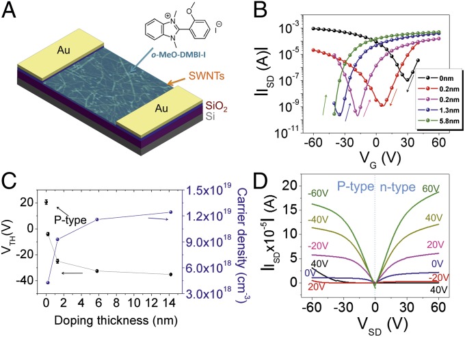
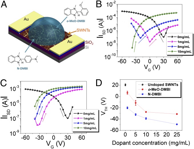
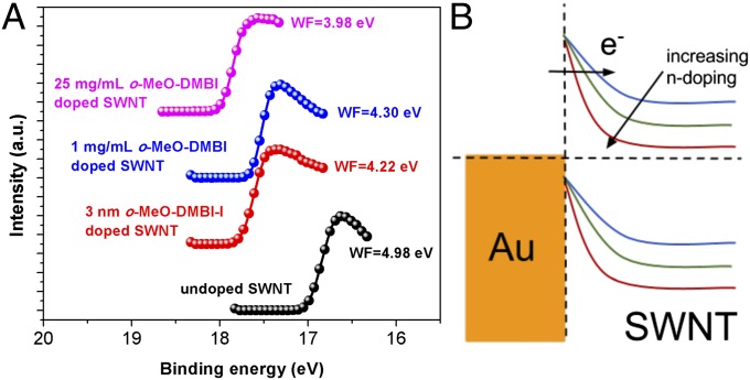
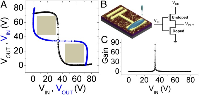
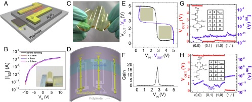
Tuning the threshold voltage of a transistor is crucial for realizing robust digital circuits. For silicon transistors, the threshold voltage can be accurately controlled by doping. However, it remains challenging to tune the threshold voltage of single-wall nanotube (SWNT) thin-film transistors. Here, we report a facile method to controllably n-dope SWNTs using 1H-benzoimidazole derivatives processed via either solution coating or vacuum deposition. The threshold voltages of our polythiophene-sorted SWNT thin-film transistors can be tuned accurately and continuously over a wide range. Photoelectron spectroscopy measurements confirmed that the SWNT Fermi level shifted to the conduction band edge with increasing doping concentration. Using this doping approach, we proceeded to fabricate SWNT complementary inverters by inkjet printing of the dopants. We observed an unprecedented noise margin of 28 V at V(DD) = 80 V (70% of 1/2V(DD)) and a gain of 85. Additionally, robust SWNT complementary metal-oxide-semiconductor inverter (noise margin 72% of 1/2VDD) and logic gates with rail-to-rail output voltage swing and subnanowatt power consumption were fabricated onto a highly flexible substrate.

Keywords: CMOS circuit; inkjet-printed; n-doping; nanomaterials.


Conflict of interest statement

The authors declare no conflict of interest.

Figures

Fig. 1.
Fig. 1.
N-doping by vacuum evaporation. (A) Schematic of vacuum-evaporated o-MeO-DMBI-I doped SWNT TFTs (L = 20 μm, W = 400 μm). (B) Transfer characteristics of SWNT TFTs doped by o-MeO-DMBI-I at different nominal thicknesses determined by a quartz crystal monitor during deposition (VSD = 80 V for n-type and VSD = −80 V for p-type). (C) Average threshold voltage and calculated carrier density as a function of o-MeO-DMBI-I thickness. Five devices were characterized for each doping thickness, with error bars showing the standard deviation (SD) from the average value. (D) Output characteristics of undoped and n-doped SWNT TFTs at an o-MeO-DMBI-I thickness of 5.8 nm.
Fig. 2.
Fig. 2.
N-doping by solution deposited dopants. (A) Schematic of o-MeO-DMBI or N-DMBI doped SWNT TFTs prepared by solution doping (L = 20 μm, W = 400 μm). Transfer characteristics of SWNT TFTs doped by (B) o-MeO-DMBI and (C) N-DMBI, at different concentrations at VSD = 80V for n-type and VSD = −80V for p-type. (D) Average threshold voltage change as a function of various o-MeO-DMBI and N-DMBI concentrations. Five devices were measured for each doping concentration, with error bars showing the SD from the average value.
Fig. 3.
Fig. 3.
(A) PES spectra of the secondary cutoff region of the undoped and doped SWNT films and their calculated work functions. (B) Schematic energy band diagram showing the electron injection barrier with increasing n-doping.
Fig. 4.
Fig. 4.
(A) VTC and noise margin extraction of o-MeO-DMBI doped SWNT complementary inverters at VDD = 80 V as prepared by inkjet printing. (B) The structure and circuit diagram of the inverter. (C) The gain of the inverter at the same VIN range.
Fig. 5.
Fig. 5.
Flexible SWNT device and circuit. (A) Schematic showing the structure of the flexible devices (L = 20 μm, W = 400 μm). (B) Transport characteristics of an n-doped device before bending and after bending at different radii of curvatures. Inset shows a digital photograph of the flexible device/circuit bent in a bending tester. (C) A digital photograph of a carbon nanotube circuit fabricated on a flexible polyimide substrate. (D) Schematic diagram of the circuit design of the flexible inverter, NAND, and NOR logic gates. (E) VTC and noise margin extraction of o-MeO-DMBI-I doped flexible SWNT complementary inverters at VDD = 5 V. (F) The gain of the inverter at the same VIN range. Output characteristics, static state currents, circuit diagrams, and truth tables of o-MeO-DMBI-I doped flexible (G) CMOS NOR and (H) CMOS NAND logic gates, at VDD = 5 V.

References

    1. Minhun J, et al. All-printed and roll-to-roll-printable 13.56-MHz-operated 1-bit RF tag on plastic foils. Electron Devices. IEEE Transactions on. 2010;57(3):571–580.
    1. Dodabalapur A. Organic and polymer transistors for electronics. Mater Today. 2006;9(4):24–30.
    1. Gelinck GH, et al. Flexible active-matrix displays and shift registers based on solution-processed organic transistors. Nat Mater. 2004;3(2):106–110. - PubMed
    1. Rogers JA, et al. Paper-like electronic displays: Large-area rubber-stamped plastic sheets of electronics and microencapsulated electrophoretic inks. Proc Natl Acad Sci USA. 2001;98(9):4835–4840. - PMC - PubMed
    1. Myny K, et al. An 8-bit, 40-instructions-per-second organic microprocessor on plastic foil. IEEE J Solid-State Circuits. 2012;47(1):284–291.

Publication types