Review
. 2014 Mar 26;26(12):1846-85.
doi: 10.1002/adma.201304496.

A review of organic and inorganic biomaterials for neural interfaces

Review

A review of organic and inorganic biomaterials for neural interfaces

Pouria Fattahi et al. Adv Mater. .

Abstract

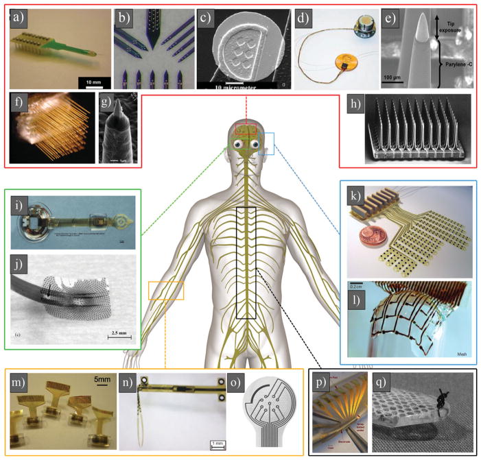
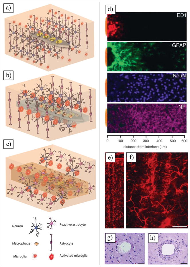
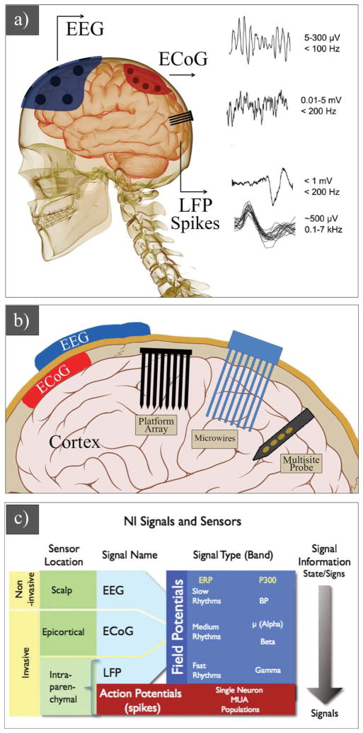
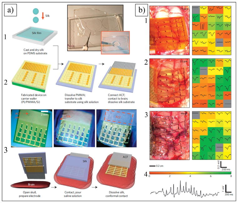
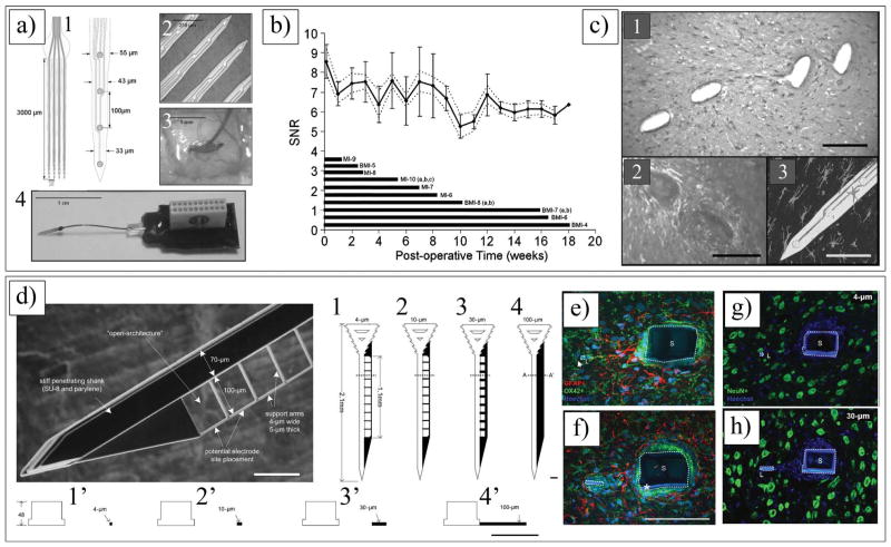
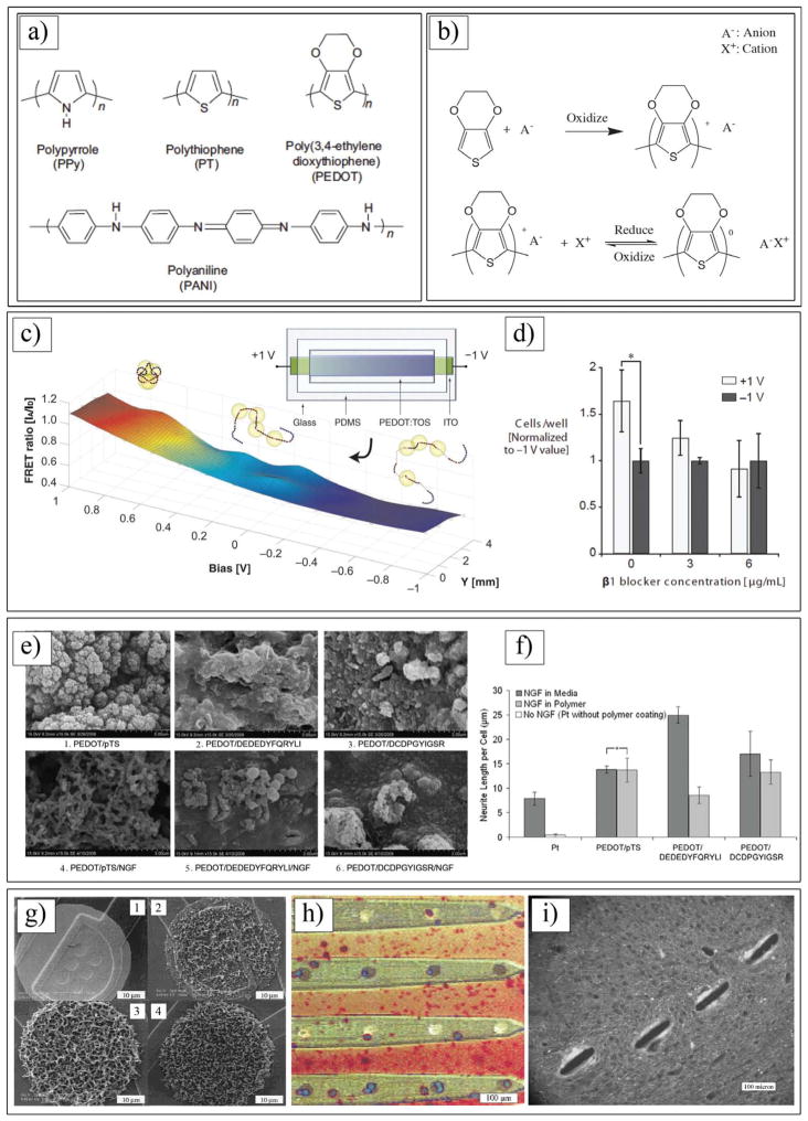
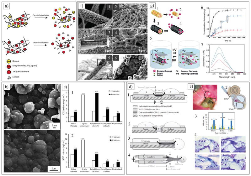
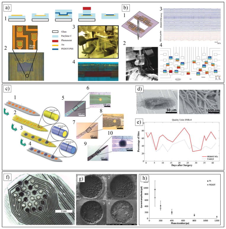
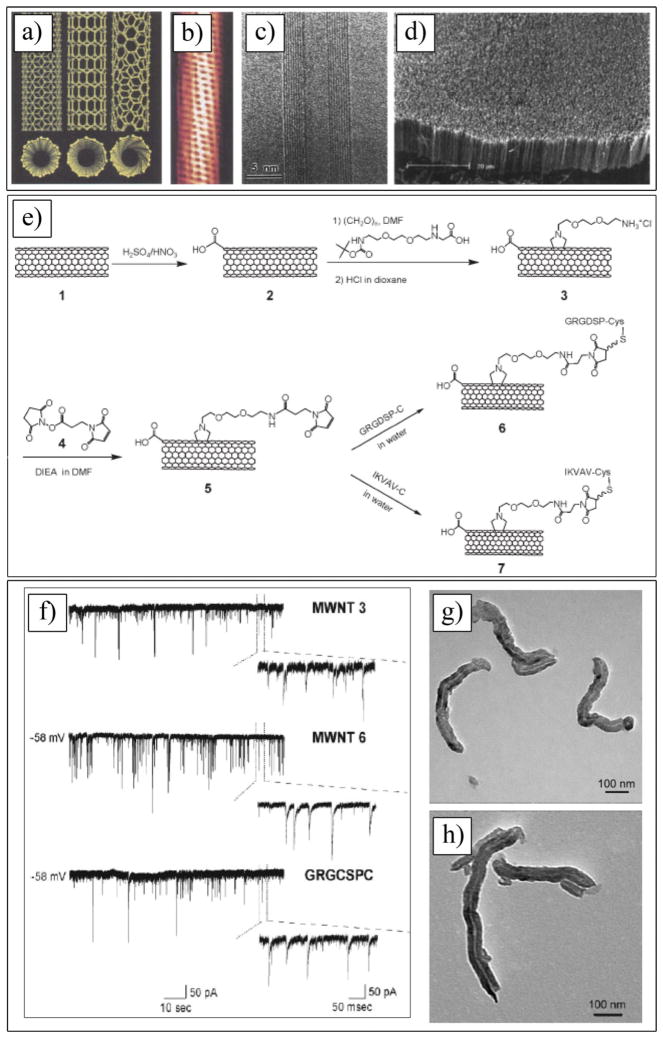
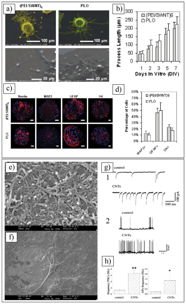
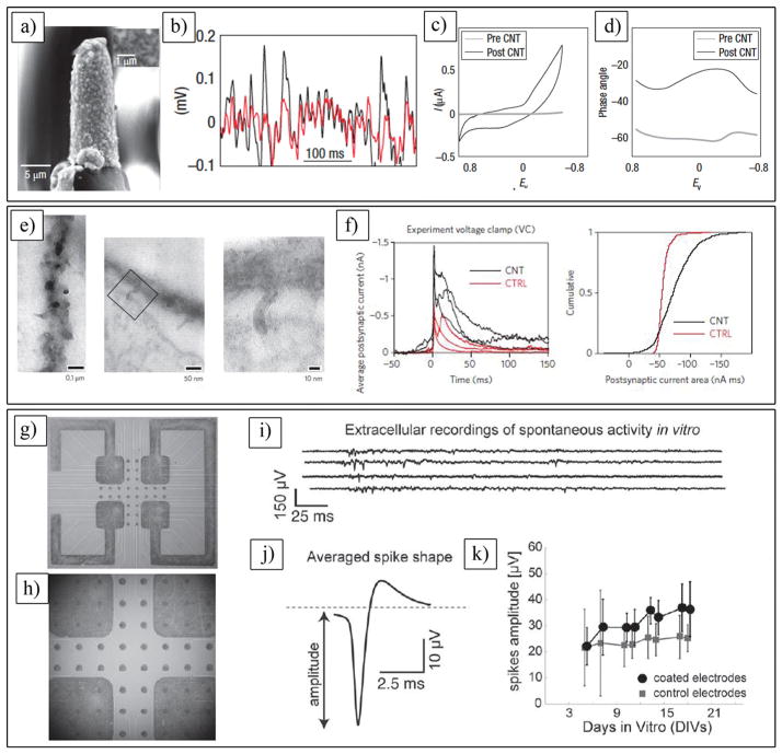
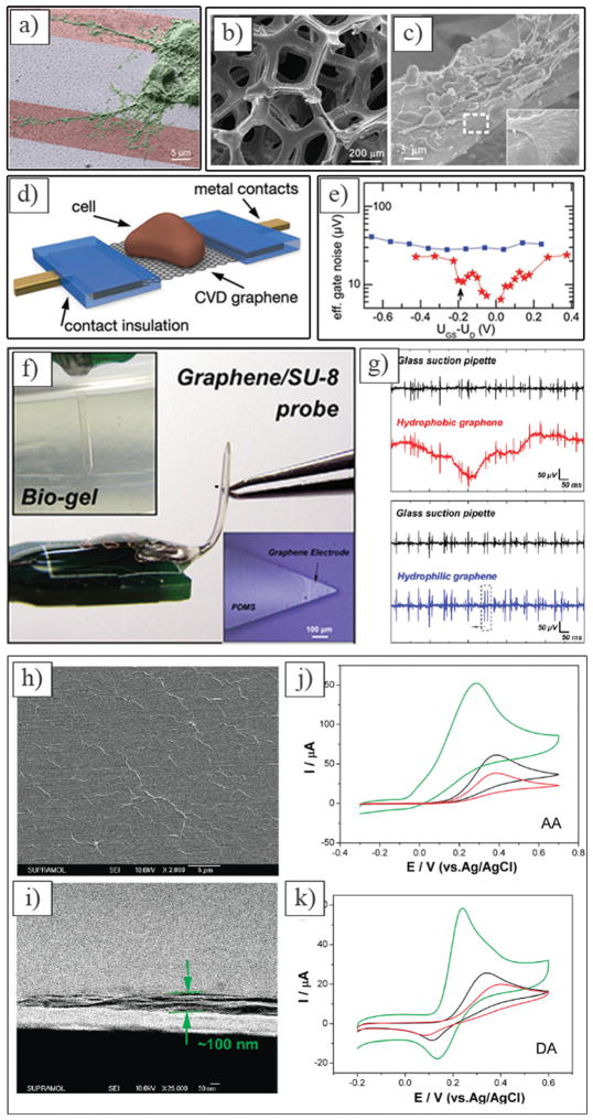
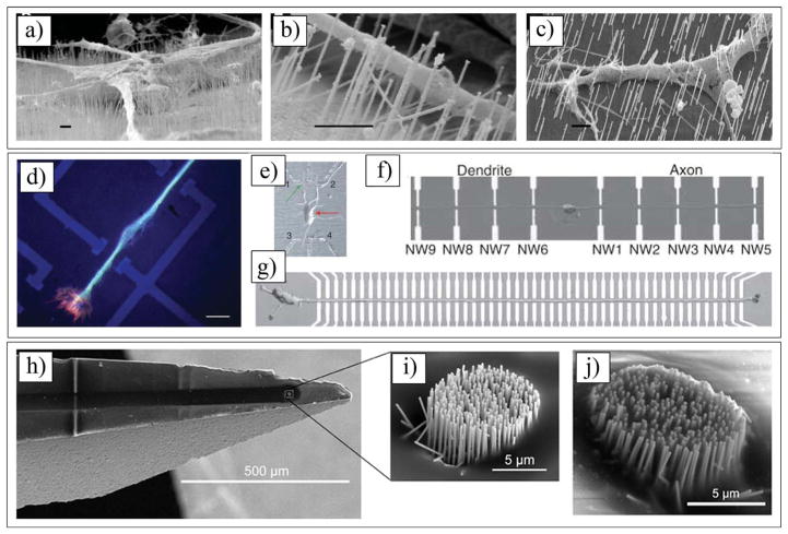
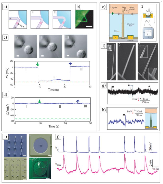
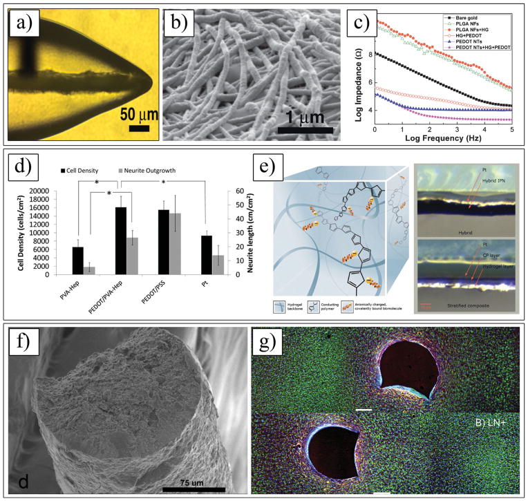
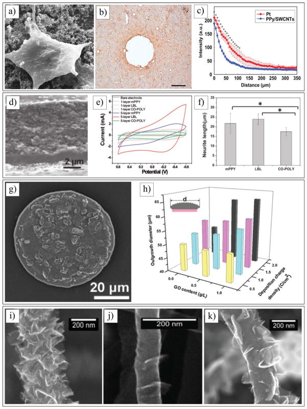
Recent advances in nanotechnology have generated wide interest in applying nanomaterials for neural prostheses. An ideal neural interface should create seamless integration into the nervous system and performs reliably for long periods of time. As a result, many nanoscale materials not originally developed for neural interfaces become attractive candidates to detect neural signals and stimulate neurons. In this comprehensive review, an overview of state-of-the-art microelectrode technologies provided fi rst, with focus on the material properties of these microdevices. The advancements in electro active nanomaterials are then reviewed, including conducting polymers, carbon nanotubes, graphene, silicon nanowires, and hybrid organic-inorganic nanomaterials, for neural recording, stimulation, and growth. Finally, technical and scientific challenges are discussed regarding biocompatibility, mechanical mismatch, and electrical properties faced by these nanomaterials for the development of long-lasting functional neural interfaces.


Figures

Figure 1
Figure 1
a) Eight-channel silicon substrate acute Michigan electrode. Reproduced with permission.[174] Copyright 2008, Elsevier. b) High-magnification photograph illustrating four different types of sites layouts for Michigan electrode (NeuroNexus Technologies). Reproduced with permission.[3] Copyright 2008, Society for Neuroscience. c) SEM image of a single gold site of Michigan electrode. Reproduced with permission.[170] Copyright 2003, Elsevier. d) BrainGate microelectrode array (i.e. Utah array) connected by a 13 cm ribbon cable to percutaneous Ti pedestal secured to skull. Reproduced with permission.[84] Copyright 2006, Nature Publishing Group. e) High-magnification image of an electrode of Utah array. Reproduced with permission.[427] Copyright, 2010, Elsevier. f) Multiple boards stacked up to form arrays with up to 128 microwires. Reproduced with permission.[414] Copyright 2003, National Academy of Sciences. g) SEM image of a microwire, showing Au tip coated with parylene. Reproduced with permission.[428] Copyright 2012, IOP Publishing. h) SEM image of 100 microelectrodes of Utah electrode array. Reproduced with permission.[84] Copyright 2006, Nature Publishing Group. i) An epiretinal vision prosthesis, final implant with parylene C and silicone rubber encapsulation. Reproduced with permission.[429] Copyright 2009, IOP Publishing.) Heat molded and annealed retinal electrode array with retained spherical curvature (arrow denotes retinal tack hole). Reproduced with permission.[430] Copyright 2008, Elsevier. k) Fully assembled electrode array. The diameter of the coin is 16 mm. Reproduced with permission.[110] Copyright 2009, IOP Publishing. l) Optical image of silk-supported polyimide electrode arrays of a 25 μm mesh wrapped onto a glass hemisphere. Reproduced with permission.[431] Copyright 2010, Nature Publishing Group. m) Schematic cross-section of the channel pattern showing the structure neutral plane (strain & 0%) at the electrode layer. Reproduced with permission.[432] Copyright, 2010 Springer. n) Transversal intrafascicular multichannel electrode. Reproduced with permission.[433] Copyright 2011, Wiley. o) Enlarged view of the sieve portion of the regenerative electrodes, with nine ring electrodes around via holes and a larger counter electrode. Reproduced with permission.[434] Copyright 2004, Elsevier. p) Fabricated PDMS-substrate MEA wrapped around a wire of similar diameter (2 mm) to that of the neonatal intact or hemisected juvenile in vitro rat spinal cord. Reproduced with permission.[435] Copyright 2008, Springer. q) Distal aspect of paddle-style epidural electrode prepared with a 3–0 suture passed and knotted through the tip. The knot serves as a fixation point for wire snare. Reproduced with permission.[436] Copyright 2011, Congress of Neurological Surgeons; published by Wolters Kluwer Health.
Figure 2
Figure 2
a) Schematic of insertion of a neural electrode inside the brain. b) Schematic of acute response to an implanted electrode. c) Schematic of chronic response to an implanted electrode. d) Immunoreactivity images using cell-type-specific markers at microelectrode brain tissue interface. Representative image collected from adjacent section of an animal with 4-week microelectrode implant illustrates general appearance of foreign body response. Position of microelectrode illustrated by orange oval (drawn to scale) left to each image. d) Reproduced with permission.[53] Copyright 2005, Elsevier. e,f) Reactive astrocytes labeled with GFAP staining encapsulate neural probes in a dense cellular sheath, Calibration bar = 50 μm. g) Acute injury caused by inserting a microelectrode into brain cortex, showing activation and migration of astrocytes and microglial cells to injury site, Calibration bar = 50 μm. h) Chronic response forming dense sheath of fibroblasts, macrophages, and astrocytes around implant, Calibration bar = 50 μm. e–h) Reproduced with permission.[97] Copyright 2010, C. Marin, E. Fernandez; published by Frontiers.
Figure 3
Figure 3
Schematic of a) neural signals (EEGs, ECoGs, LFPs, and spikes) and their properties. b) EEG electrode on the skull, ECoG electrode on the surface of brain, and penetrating electrodes: three main types of intraparenchymal (intracortical) sensors now in use are illustrated: platform array, an array of electrodes emanating from a substrate that rests on the cortical surface; multisite probe, with contacts along a flattened shank; and microwire assemblies, consisting of fine wires. c) Signals and sensors for neural interface systems. c) Reproduced with permission.[88] Copyright 2008, Elsevier.
Figure 4
Figure 4
a) Schematics and images showing fabricating steps for conformal silk-supported PI electrode arrays. a1) Casting and drying of silk fibroin solution on temporary PDMS substrate. a2) Fabricating steps for electrode arrays. a3) Schematics of clinical use of a representative device in ultrathin mesh geometry with dissolvable silk support. b) Photos and data from animal validation experiments. b1–b3) Images of electrode array on a feline brain (left) and average evoked response from each electrode (right) with color showing ratio of root mean square (rms) amplitude of each average electrode response in 200 ms window (plotted) immediately preceding the stimulus presentation for a 76 μm (b1), 2.5 μm (b2) and 2.5 μm mesh (b3) electrode array. Color bar at bottom of (b3) provides scale used in right frames of b1–b3 to indicate rms amplitude ratios. b4) Representative voltage data from a single electrode in 2.5 μm mesh electrode array showing a sleep spindle. a,b) Reproduced with permission.[431] Copyright 2010, Nature Publishing Group.
Figure 5
Figure 5
a) Michigan 16-channel probe. a1) Schematic of four shanks. a2) Four shank, 16-channel probe with 20 μm diameter-recording sites. a3) Implanted probe in auditory cortex. Thin layer of ALGEL covers implanted probe and surface of the brain. a4) Assembled probe. b) Average percent of active electrodes on implanted arrays. Time bars at bottom of figure represent each animal’s contribution to mean results. c) c1) 20 μm H&E stained section from a four-shank device implanted in animal for 127 days. c2) 50 μm immunostained section (GFAP and laminin) showing a close-up of two shanks from four-shank device implanted in animal for 36 days. c3) 150 μm section taken parallel to a probe with a single shank remaining intact within the section for 38 days. Calibration bar = 100 μm. a–c) Reproduced with permission.[17] Copyright 2004, Institute of Electrical and Electronics Engineers. d) SEM image of a parylene-based open-architecture probe used for in vivo testing. d1–d4) CAD drawings of each probe design indicating overall length and width of three lattice platforms (4, 10, 30 μm), and d4) one nonlattice platform (100 μm wide). d12–d42) Crosssectional view of line A–A2 shown in (d1–d4). All the probes have identical shank and outer dimensions. Calibration bar = 100 μm. e,f) Expression of astrocytes (dyed with red GFAP stain), microglia (dyed with green OX-42 protein stain), and cell nuclei (dyed with blue Hoechst 33342 stain) of parylene electrode implanted in the rat brain. Calibration bar = 100 μm. g,h) IHC images showing NeuN + reactivity (green) and Hoechst counterstain (blue) for each probe type. Shank marked with S and much smaller lateral edge marked with L. Calibration bar = 100 μm. d–h) Reproduced with permission.[113] Copyright 2007, Elsevier.
Figure 6
Figure 6
a) Chemical structures of various conducting polymers. b) Electrochemical polymerization of PEDOT and redox behavior of PEDOT doped with motile anion A. c) FRET (Förster Resonance Energy Transfer) ratios on gradient devices as a function of applied bias and position. d) Relative number of adhered 3T3-L1 mouse fibroblasts on fully oxidized (+1 V) and reduced (–1 V) pixels, for varying doses of a β1 function-blocking antibody. c,d) Reproduced with permission.[190] Copyright 2012, Wiley-VCH. e) SEM images at 15,000×magnification of NGF entrapped in PEDOT films compared with control films produced without NGF modification of the electrolyte. f) Neurite outgrowth of PC12 cells on laminin peptide-doped PEDOT with NGF incorporation at 96 h post-plating. Neurite outgrowth is represented as neurite length per adhered cell, calculated by normalizing total neurite length to cell density. Standard error of mean is given (n = 3). *No significant difference. e,f) Reproduced with permission.[36] Copyright 2010, Elsevier. g) SEM images of Ppy/SLPF-coated electrode sites. From g1) to g4), deposition time increased, corresponding to a total charge passed of (g1) 0 μC, (g2) 1 μC, (g3) 4 μC and (g4) 10 μC. Area of uncoated electrode site is 1250 μm2. Reproduced with permission.[168] Copyright 2001, Wiley. h) Ppy/SLPF coated 4-shank 16-channel neural probe cultured with rat glial cells. Dark black spots are coated electrode sites and bright ones are uncoated. i) Neurofilament immunostained tissue sections of guinea pig brain where 4-shank Ppy/DCDPGYIGSR coated probes were implanted and pulled out after 3 weeks. h,i) Reproduced with permission.[35] Copyright 2003, Elsevier.
Figure 7
Figure 7
a) Schematic of incorporation and controlled release of drugs and biomolecules as dopants or non-doping inclusion in CPs. b) SEM images of Ppy/pTS/NT-3 films (b1) before and (b2) after 60 min electrical stimulation in 0.9% NaCl solution. c) Mass of NT-3 released from a (c1) thin (3.6 μm) and (c2) thick (26 μm) Ppy/pTS/NT-3 polymer films in 1mL of 0.9% NaCl by various electrochemical release methods. b,c) Reproduced with permission.[213] Copyright 2006, Elsevier. d) Planar and encapsulated geometries of delivery device. d1) Side view of planar device used in initial Glu, Asp and GABA transport studies. Black arrow indicates flow of charged neurotransmitters from source electrolyte, S, through anode, then through over-oxidized channel and finally out into target electrolyte, T, through cathode. d2) Side view showing developmental progression from planar device (d1), d3) Side-view scheme of encapsulated device. d4) Top view of encapsulated device with electrolyte reservoir tubes 2 mm in outer diameter. e) In vivo application of ion pump. e1) Photograph of device mounted on RWM, with two ion channels visible as dark blue strips on transparent substrate. e2) Experimental scheme. e3) Mean ABR shift (re:pre-treatment thresholds) as a function of recording frequency after 15 min (hatched bars) and 60 min (filled bars) of Glu (blue) and HC (yellow) delivery. Frequencies are illustrated in relation to their increasing distance from RWM. Error bars indicate standard deviation. e4) Histological sections of cochlea with inner hair cells on right and outer hair cells on left showing (i) effect of HC delivery (as control) and (ii) effect of Glu delivery (excitotoxic-induced damage to auditory dendrites indicated with asterisks) in lower basal region (turn 1), and similar (iii) HC and (iv) Glu effect in upper basal region (turn 2). Calibration bar = 20 μm. d,e) Reproduced with permission.[166] Copyright 2009, Nature Publishing Group. f) SEM images of PLGA nanofibers and PEDOT nanotubes. f1) Diameters of the PLGA fibers range 40–500 nm. f2) Electropolymerized PEDOT nanotubes on electrode site of an acute neural probe tip after removing the PLGA core fibers. f3) A section of f2) cut with a FIB showing silicon substrate layer and PEDOT nanofiber coating. f4) Higher-magnification image of f3) showing PEDOT nanotubes crossing each other. f5) PEDOT nanotube. f6) Higher-magnification image of PEDOT nanotube. g) Schematics of controlled release of dexamethasone: g1) dexamethasone-loaded electrospun PLGA, g2) hydrolytic degradation of PLGA fibers leading to release of drug, and g3) electrochemical deposition of PEDOT around dexamethasone loaded electrospun PLGA fiber slows down release of dexamethasone. g4) PEDOT nanotubes in a neutral electrical condition. g5) External electrical stimulation controls the release of dexamethasone from the PEDOT nanotubes due to contraction or expansion of the PEDOT. g6) Cumulative mass release of dexamethasone from: PLGA nanofibers (black squares), PEDOT-coated PLGA nanofibers (red circles) without electrical stimulation, and PEDOT-coated PLGA nanofibers with electrical stimulation of 1 V applied at five specific times indicated by circled data points (blue triangles). g7) UV absorption of dexamethasone-loaded PEDOT nanotubes. f,g) Reproduced with permission.[173] Copyright 2006, Wiley-VCH.
Figure 8
Figure 8
a) a1) Schematic representation of the fabrication process indicating the cross-section of an electrode (not to scale). a2) Microscopy images of the array and a detailed view of three electrodes. a3) The electrode array is shown to support the weight of a quartz wafer a4) to conform to a cylinder with a radius of 2.2 mm. b) b1) Schematic of the experiment used for the validation of the PEDOT:PSS array with a silicon probe viewed from inside the brain. b2) photograph showing the implantation. b3) Recordings from 25 electrodes in the PEDOT:PSS array, and from 10 electrodes in the silicon probe, ordered from superficial to deeper in the cortex. b4) Time-frequency (TF) analysis of the signals recorded by a few electrodes (black frames, X-axis: time, 10 min; y-axis: frequency, 0.1–50 Hz; color coding: power, dB) and their cross-spectrum coherences (open boxes, same axes as TF plots, color coding: coherence). a,b) Reproduced with permission.[95] Copyright 2011, Wiley-VCH. c) Schematic illustration of PEDOT nanotube fabrication on neural microelectrodes: c1, c2) Electrospinning of biodegradable PLLA template fibers. c3) Electrochemical deposition of PEDOT. c4) dissolving the electrospun core fibers to create conducting polymer nanotubes. c5-c10) Optical microscopy images of the entire microelectrode (c5) and single electrode site (c6) before surface modification. (c7) and single electrode site (c8) after electrospinning of PLLA nanofibers. (c9) and single electrode site (c10) after electrochemical deposition of PEDOT and removing the PLLA core fibers. d) PEDOT nanotubes on the surface of a single microelectrode site. Right image is a higher magnification of left image. e) Percentage of sites recording low-and high-quality units. PEDOT nanotube sites demonstrated a significant improvement in percentage of sites recording high-quality units on a day-to-day basis. f) 24-electrode array in hexagonal (hex) configuration used for in vivo studies with 12 bare Pt (light electrode sites) and 12 PEDOT/pTS-coated electrodes (dark electrodes). g) SEM images of g1) active PEDOT (prior to stimulation), g2) active PEDOT (after stimulation), g3) passive PEDOT (prior to stimulation) and g4) passive PEDOT (after stimulation). c–g) Reproduced with permission.[32] Copyright 2009, Wiley-VCH. h) Strength vs duration curve, demonstrating the relationship between average current required to reach threshold and duration of phases for biphasic current driven stimulation of tissue using suprachoroidal electrodes (n = 5). h,j) Reproduced with permission.[156] Copyright 2013, IOP Publishing.
Figure 9
Figure 9
a) Schematic illustrations of the structures of armchair, zigzag, and chiral SWCNTs. Projections normal to the tube axis and perspective views along the tube axis are on the top and bottom, respectively. b) Tunneling electron microscope image showing the helical structure of a 1.3-nm-diameter chiral SWCNT. c) TEM image of a MWCNT containing a concentrically nested array of nine SWCNTs. d) SEM image of an array of MWCNTs grown as a nanotube forest. a–d) Reproduced with permission.[227] Copyright 2002, American Association for the Advancement of Science. e) Synthesis of MWNT–peptide conjugates. f) MWCNTs 3, 6, and peptide GRGDSPC (Pep 1) alone do not affect neuronal survival and activity. Tracings represent spontaneous synaptic activity recorded from neurons (8 days in vitro) after MWCNTs 3, 6, and GRGDSPC incubation at 24 h washout. Below each recording, on the right, the magnifications show the presence of heterogeneous events (inward currents), representing the activation of mixed synapses impinging on the recorded neurons. g,h) TEM images of MWCNTs 2, and 7. e–h) Reproduced with permission.[437] Copyright 2009, Wiley-VCH.
Figure 10
Figure 10
a) Color-enhanced SEM images highlighting neurite outgrowth of differentiated neurospheres on day 7 (first row). SEM images at higher magnification showing migrating NSCs around neurospheres (second row). b) Evaluation of the lengths of processes extending from the differentiated neurospheres for the 7 day culture period. c) Confocal microscopy images differentiated neurospheres on day 7. Neurospheres were stained for markers of NSCs (nestin), neurons (MAP2), astrocytes (GFAP), and oligodendrocytes (O4). Neural markers are shown in red, while the cell nuclei, counterstained with DAPI, are shown in blue. Images represent scans near the center of the neurospheres. Calibration bar = 20 μm. d) Average percentages of differentiated cell phenotypes after 7 days in culture. a–d) Reproduced with permission.[241] Copyright 2007, ACS Publications. e) SEM image showing the retention on glass of MWCNT films after an 8-day test in culturing conditions. f) Neonatal hippocampal neuron growing on dispersed MWCNT after 8 days in culture. The surface structure, composed of films of MWCNT and peptide-free glass, allows neuron adhesion. Dendrites and axons extend across MWCNT, glial cells, and glass. g) CNT substrate increases hippocampal neurons spontaneous synaptic activity and firing. g1) Spontaneous synaptic currents (PSCs) are shown in both control (top tracings) and in cultures grown on CNT substrate (bottom tracings). g2) Current clamp recordings from cultured hippocampal neurons in control (top tracings) and CNT growth conditions (bottom tracings). Spontaneous firing activity is greatly boosted in the presence of CNT substrates. h) Histogram plots of PSCs-(left) and APs-(right) frequency in control and CNT cells; note the significant increase in the occurrence of both events when measured in CNT cultures. **P < 0.0001 and *P < 0.05. e–h) Reproduced with permission.[127] Copyright 2005, ACS Publications.
Figure 11
Figure 11
a) CNTs covalently attached to a sharp tungsten electrode. b) Local field potential traces from bare controls (red trace) and CNT-coated (black trace) electrodes show correlated activity but larger amplitude responses from CNT-coated electrodes. c,d) Covalent coating of CNTs increased the charge transfer (c) and decreased the phase angle (d). a–d) Reproduced with permission.[28] Copyright 2008, Nature Publishing Group. e) 1) Morphology of nanotubes. 2,3) High-magnification micrographs from a section consecutive. The rectangular area in 2 is magnified in 3. f) average spontaneous postsynaptic currents waveforms in six neurons were computed to provide a measure of the probability of presynaptic event clustering (that is, a burst of spikes), within a window of 50–150 ms around its peak. Significant differences in the postsynaptic currents duration are apparent from the shift in the empirical cumulative distributions of their areas. e,f) Reproduced with permission.[29] Copyright 2009, Nature Publishing Group. g,h) Optical microscopy images of titanium nitride (TiN) microelectrode arrays printed by functionalized COOH–MWCNTs. Stamps of arbitrary shape were designed in this case to cover single electrodes and connect them together. i) Extracellular raw voltage waveforms as detected by four MEA electrodes in long-term neuronal culturing experiments. Each recording channel independently captures extracellular action potentials or j) “spikes”, spontaneously fired by neurons growing in proximity of the microelectrode. k) Comparing the average amplitude of the extracellular spikes detected across several days by MEA electrodes coated by CNTs to those detected by uncoated electrodes reveals, on average, much higher signal amplitudes, which are attributed to the improved electrical properties at the electrode–electrolyte interface and the resulting signal-to-noise ratio. g–k) Reproduced with permission.[291] Copyright 2011, Wiley-VCH.
Figure 12
Figure 12
a) SEM image with graphene regions colored in red, corresponds to the region of the 3-cell aggregate marked in green. Reproduced with permission.[438] Copyright 2013, Wiley-VCH. b) SEM micrographs of 3D-Graphenes (GFs). c) High magnified SEM images of NSCs cultured on 3D-GFs under the proliferation medium. The inset illustrates the interaction between the cell filopodia and 3D-GF surface. b,c) Reproduced with permission.[439] Copyright 2013, Nature Publishing Group. d) Schematic of a G-SGFET with a cell on the gate area. The graphene is shown between the drain and source metal contracts, which are protected by a chemically resistant layer. e) Effective gate noise of a graphene (red stars) and a silicon SGFET (blue squares). UD refers to the UGS (gate voltage) at which the minimum of the current is observed. The arrow marks the point of maximum transductance. d,e) Reproduced with permission.[297] Copyright 2011, Wiley-VCH. f) Optical micrograph of a flexible microprobe bent through 90 degree configurations and penetrating an agar gel. Inset shows graphene electrode upon the SU-8 substrate. g) Extracellular signals with a larger SNR were recorded with a graphene electrode after steam plasma treatment. f,g) Reproduced with permission.[298] Copyright 2013, Elsevier. h,i) SEM images of the CR-GO/GC electrode (h and i). j,k) CVs for 3 mM AA (j) and DA (k) at CR-GO/GC (green), graphite/GC (red), and GC electrodes (black). Electrolyte: 0.1 M pH 7.0 PBS. Scan rate: 50 mV s−1. h–k) Reproduced with permission.[440] Copyright 2009, ACS Publications.
Figure 13
Figure 13
Images a–c demonstrate three different types of process growth. a) Processes growing on top of wires, attached to their tips. b) Axon growing in space between substrate and wire tips, adhering to sides of wires. c) Process spreading over bulk substrate, apparently engulfing nanowires encountered along its path. Scale bars 1 μm. a–c) Reproduced with permission.[375] Copyright 2007, ACS Publications. d) Neuritic guidance on SiNW-FETs. Microtubules staining (anti-tyrosinated tubulin, green) reveals neurite shaft and F-actin labeling (phalloidin, red) shows growth cone at neurite tip. Calibration bar = 5 μm. Reproduced with permission.[376] Copyright 2012, Wiley-VCH. e) Optical image of a cortex neuron connected to three of four functional NW devices in array. f) Optical image of a cortex neuron with axon and dendrite aligned in opposite directions. g) Optical image of aligned axon crossing an array of 50 NW devices with a 10-μm interdevice spacing. e–g) Reproduced with permission.[364] Copyright 2006, American Association for the Advancement of Science. h) SEM image of the nanowire-based electrode tip. i) SEM image of nanowire-based sensing region made with an array of freestanding vertical gallium phosphide nanowires covered with hafnium oxide and metal film. j) SEM image of sensing site presented after multiple implantations into rat cortex. h–j) Reproduced with permission.[31] Copyright 2013, Suyatin et al.; published by PLOS ONE.
Figure 14
Figure 14
Surface modification and cellular entry. a) Schematics of nanowire probe entrance into a cell. Dark purple, light purple, pink, and blue colors denote phospholipid bilayers, heavily doped nanowire segments, active sensor segment, and cytosol, respectively. b) False-color fluorescence image of a lipidcoated nanowire probe. c) Differential interference contrast microscopy images (top) and electrical recording (bottom) of an HL-1 cell and 60° kinked nanowire probe as cell approaches (I), contacts and internalizes (II), and is retracted from (III) nanoprobe. A pulled-glass micropipette (inner tip diameter ≈ 5 μm) was used to manipulate and voltage clamp HL-1 cell. Dashed green line corresponds to micropipette potential. Calibration bar = 5 μm. d) Electrical recording with a 60° kinked nanowire probe without phospholipids surface modification. Green and blue arrows in (c) and (d) mark beginnings of cell penetration and withdrawal, respectively. a–d) Reproduced with permission.[441] Copyright 2010, American Association for the Advancement of Science. e) Schematic diagrams showing (left) a cell coupled to a BIT-FET and variation in device conductance G (right) with time t during an action potential Vm. S and D indicate source and drain electrodes. f1) SEM image of a germanium nanowire branch on a silicon nanowire oriented close to surface normal. Inset: gold nanodot on a silicon nanowire before growth of germanium nanowire. f2) SEM image of a germanium/silicon heterostructure coated with ALD SiO2. f3) SEM image of a final nanotube on a silicon nanowire. Insets: magnified images of top and bottom of nanotube. Calibration bar = 100 nm (inset of b), 200 nm (all other images). g) Magnified view of Representative trace (conductance versus time) reflecting transition from extracellular to intracellular recording. h) Magnified view of trace inside blue dashed rectangle in (g). Stars in (g) and (h) mark position of extracellular spikes. e–h) Reproduced with permission.[353] Copyright 2012, Nature Publishing Group. i1) SEM image of nine silicon nanowires that constitute active region of a VNEA. Calibration bar = 1 μm. i2) SEM image of a VNEA pad. False coloring indicates additional insulation from Al2O3 (green). Calibration bar = 10 μm. i3) SEM image of a device consisting of 16 stimulation/recording pads for parallel multi-site interrogation of neuronal circuits. Calibration bar = 120 μm. i4) Representative DIC micrograph of a rat cortical neuron cultured on a VNEA pad (6 DIV). Calibration bar = 20 μm. j) Action potentials were stimulated using a patch pipette (blue) and recorded by the VNEA pad in Faradaic mode (magenta). i,j) Reproduced with permission.[442] Copyright 2012, Nature Publishing Group.
Figure 15
Figure 15
a) Side view of optical micrograph of deposited PEDOT on electrode site showing vertical growth of PEDOT from an electrode site and through the alginate hydrogel scaffold (black color). b) SEM image of electrode site after dissolving the alginate coating and electrospun nanofibers. This image reveals that PEDOT was grown around the electrospun nanofibers to form PEDOT nanotubes. c) EIS of bare gold (black squares), PLGA NFs (green hollow triangles), PLGA NFs+HG (orange circles), HG+PEDOT (red hollow circles), PEDOT NTs (blue triangles), and PEDOT NTs+HG+PEDOT (pink stars), with the applied deposition charge density was 2.88 C cm−2. a–c) Reproduced with permission.[38] Copyright 2009, Wiley-VCH. d) PC12 cell density and neurite outgrowth are shown with standard deviation (N = 3, * p < 0.05). e) Schematic of ideal hybrid configuration (left) and photo comparison of hybrid material created from using a bound dopant, compared to stratified composite produced from using a free dopant (right). Both material samples are hydrated. d,e) Reproduced with permission.[39] Copyright 2012, Wiley-VCH. f) Cross section of CNT/Agarose fiber. g) Representative immunohistochemical images of fibers inserted into rat cortex. top) non-laminin functionalized fiber, down) laminin functionalized fiber, yellow – astrocytes (GFAP). blue – microglia (Iba-1). green – neurons (Nissl). Calibration bar = 100 μm. f,g) Reproduced with permission.[443] Copyright 2011, Wiley-VCH.
Figure 16
Figure 16
a) SEM image of PC12 cells cultured on Ppy/SWCNT deposited ITO substrate in the presence of 50 mg mL−1 NGF at day 7. Calibration bar = 5 μm. b) Astrocyte response was evaluated using GFAP immunostaining for PPy/SWCNT deposited Pt implant after 6 weeks post-implantation. c) Quantitative comparison of GFAP immunoreactivity between the control and deposited implants was made via GFAP intensity profiles as a function of distance from the implant interface. a–c) Reproduced with permission.[444] Copyright 2010, Elsevier. d) SEM image of cross-sectional view of multilayered Ppy/MWCNT, the thickness is 7.53 ± 0.21 μm. e) CV measurement of multilayered Ppy, LBL, and CO-POLY. f) Average neurite length per cell in PC12 cells treated with NGF for three days (n ≥ 3). d-f) Reproduced with permission.[445] Copyright 2011, RSC Publishing. g) FESEM image of electrochemically deposited Ppy/GO (Prepared with 1.0 g L−1 GO in aqueous solution) coating on Pt electrode site with fixed deposition charge density of 1.5 C cm−2. h) Chart of outgrowth diameters of different PPy/GO coatings as a function of GO content and deposition charge density. g,h) Reproduced with permission.[446] Copyright 2011, Elsevier. i–k) SEM images of graphenated carbon nanotubes (g-CNTs). Low-density graphene foliates on a CNT (i). Medium-density graphene foliates on a CNT (j). High-density graphene foliates on a CNT (k). Structures were reproducible and observed over several square centimeters after microwave plasma chemical vapor deposition growth. i-k) Reproduced with permission.[412] Copyright 2012, Materials Research Society/Cambridge University Press.

Similar articles

Cited by

References

    1. Nicolelis MA. Nat Rev Neurosci. 2003;4:417. - PubMed
    1. Schwartz AB, Cui XT, Weber DJ, Moran DW. Neuron. 2006;52:205. - PubMed
    1. Kipke DR, Shain W, Buzsaki G, Fetz E, Henderson JM, Hetke JF, Schalk G. J Neurosci. 2008;28:11830. - PMC - PubMed
    1. Hatsopoulos NG, Donoghue JP. Annu Rev Neurosci. 2009;32:249. - PMC - PubMed
    1. Marg E, Adams JE. Electroencephalography and Clin Neurophysiol. 1967;23:277. - PubMed

Publication types

Substances