

Low-cost flexible thin-film detector for medical dosimetry applications
- PMID: 24710432
- PMCID: PMC5875488
- DOI: 10.1120/jacmp.v15i2.4454
Low-cost flexible thin-film detector for medical dosimetry applications
Abstract
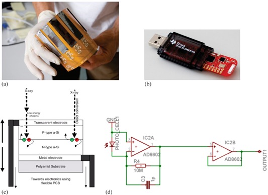
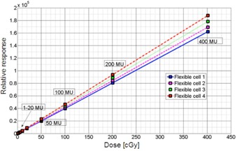
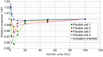
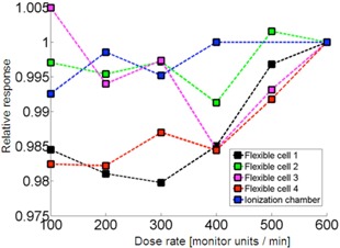
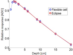
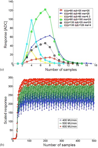
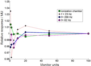
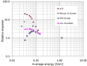
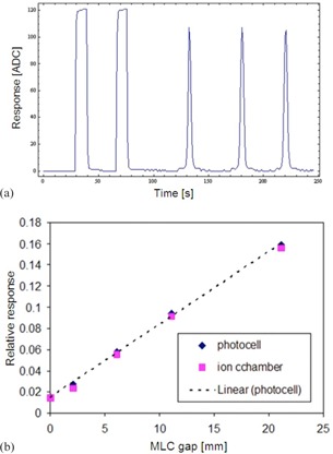
The purpose of this study is to characterize dosimetric properties of thin film photovoltaic sensors as a platform for development of prototype dose verification equipment in radiotherapy. Towards this goal, flexible thin-film sensors of dose with embedded data acquisition electronics and wireless data transmission are prototyped and tested in kV and MV photon beams. Fundamental dosimetric properties are determined in view of a specific application to dose verification in multiple planes or curved surfaces inside a phantom. Uniqueness of the new thin-film sensors consists in their mechanical properties, low-power operation, and low-cost. They are thinner and more flexible than dosimetric films. In principle, each thin-film sensor can be fabricated in any size (mm² - cm² areas) and shape. Individual sensors can be put together in an array of sensors spreading over large areas and yet being light. Photovoltaic mode of charge collection (of electrons and holes) does not require external electric field applied to the sensor, and this implies simplicity of data acquisition electronics and low power operation. The prototype device used for testing consists of several thin film dose sensors, each of about 1.5 cm × 5 cm area, connected to simple readout electronics. Sensitivity of the sensors is determined per unit area and compared to EPID sensitivity, as well as other standard photodiodes. Each sensor independently measures dose and is based on commercially available flexible thin-film aSi photodiodes. Readout electronics consists of an ultra low-power microcontroller, radio frequency transmitter, and a low-noise amplification circuit implemented on a flexible printed circuit board. Detector output is digitized and transmitted wirelessly to an external host computer where it is integrated and processed. A megavoltage medical linear accelerator (Varian Tx) equipped with kilovoltage online imaging system and a Cobalt source are used to irradiate different thin-film detector sensors in a Solid Water phantom under various irradiation conditions. Different factors are considered in characterization of the device attributes: energies (80 kVp, 130 kVp, 6 MV, 15 MV), dose rates (different ms × mA, 100-600 MU/min), total doses (0.1 cGy-500 cGy), depths (0.5 cm-20 cm), irradiation angles with respect to the detector surface (0°-180°), and IMRT tests (closed MLC, sweeping gap). The detector response to MV radiation is both linear with total dose (~1-400 cGy) and independent of dose rate (100-600 Mu/min). The sensitivity per unit area of thin-film sensors is lower than for aSi flat-panel detectors, but sufficient to acquire stable and accurate signals during irradiations. The proposed thin-film photodiode system has properties which make it promising for clinical dosimetry. Due to the mechanical flexibility of each sensor and readout electronics, low-cost, and wireless data acquisition, it could be considered for quality assurance (e.g., IMRT, mechanical linac QA), as well as real-time dose monitoring in challenging setup configurations, including large area and 3D detection (multiple planes or curved surfaces).
Figures

References
-
- Leroy C, Rancoita P. Principles of radiation interaction in matter and detection. Singapore: World Scientific Publishing Company; 2009.
-
- Herman MG, Balter JM, Jaffray DA, et al. Clinical use of electronic portal imaging: report of AAPM Radiation Therapy Committee Task Group 58. Med Phys. 2001;28(5):712–37. - PubMed
-
- Antonuk LE. Electronic portal imaging devices: a review and historical perspective of contemporary technologies and research. Phys Med Biol. 2002;47(6):31–65. - PubMed
-
- Yoo S, Kim GY, Hammoud R, et al. A quality assurance program for the on‐board imager. Med Phys. 2006;33(11):4431–47. - PubMed
Publication types
MeSH terms
LinkOut - more resources
Full Text Sources
Other Literature Sources
Research Materials
Miscellaneous
