. 2014 Jun 24;8(6):5395-401.
doi: 10.1021/nn501459v. Epub 2014 May 2.

Imaging and tuning molecular levels at the surface of a gated graphene device

Affiliations

Imaging and tuning molecular levels at the surface of a gated graphene device

Alexander Riss et al. ACS Nano. .

Abstract

Gate-controlled tuning of the charge carrier density in graphene devices provides new opportunities to control the behavior of molecular adsorbates. We have used scanning tunneling microscopy (STM) and spectroscopy (STS) to show how the vibronic electronic levels of 1,3,5-tris(2,2-dicyanovinyl)benzene molecules adsorbed onto a graphene/BN/SiO2 device can be tuned via application of a backgate voltage. The molecules are observed to electronically decouple from the graphene layer, giving rise to well-resolved vibronic states in dI/dV spectroscopy at the single-molecule level. Density functional theory (DFT) and many-body spectral function calculations show that these states arise from molecular orbitals coupled strongly to carbon-hydrogen rocking modes. Application of a back-gate voltage allows switching between different electronic states of the molecules for fixed sample bias.


Figures
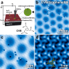
Figure 1
Figure 1
CVB molecules on a graphene/BN/SiO2 FET device. (a) Sketch of the back-gated graphene device used in these STM/STS measurements, as well as a model of the CVB molecule. (b–d) STM images of a monolayer of CVB molecules on graphene/BN show the hexagonal lattice of the CVB molecules at different zoom values (VS = 2.0 V, It = 10 pA, T = 4 K). Isolated vacancies are observed in (b) and (c).
Figure 2
Figure 2
STM spectroscopy of CVB/graphene/BN reveals vibronic response. (a) dI/dV spectrum measured with STM tip held above a monolayer of CVB molecules on a graphene/BN FET device (VG = 0). Spectrum is featureless over the range −0.5 V < VS < 1.6 V but shows four clear molecule-induced resonances (marked 1–4) in the range 1.6 V < VS < 2.8 V (junction set-point parameters VS = 2.7 V, It = 160 pA; the spectrum is normalized by its value at 2.6 V). Inset shows a section of the dI/dV spectrum over the range −0.6 V < VS < 0.6 V where the tip has been lowered by 4 Å relative to other spectra (junction set-point parameters: VS = 0.6 V, It = 40 pA; tip is closer because VS now lies in the HOMO–LUMO gap). Here the Dirac point can be observed at VS ≈ 0 V (VG = 0 V). Inset also shows onset of peak 1 (0.6 V < VS < 1.9 V) for typical junction set-point parameters: VS = 1.9 V, It = 40 pA. Peaks 1 and 4 are interpreted as LUMO and LUMO+1, respectively, while peaks 2 and 3 are interpreted as vibronic satellites of the LUMO (see text). (b) Experimental dI/dV maps obtained at voltages VS = 1.85, 2.4, and 2.65 V (VG = 0 V). dI/dV maps taken in the range 1.85 V < VS < 2.4 V probe the local density of states (LDOS) of peaks 1–3 and look very similar. The dI/dV map taken at VS = 2.65 V probes peak 4 and yields a LDOS pattern that is different from the pattern observed for peaks 1–3. (c) Calculated density of states (DOS) of vibrational modes of CVB molecules on graphene (gray lines), as well as the electron–phonon coupling strength between the CVB vibrational modes and the CVB LUMO state (vertical blue lines). The blue curve shows the calculated electron–phonon coupling broadened with a Gaussian function of width 16 meV.
Figure 3
Figure 3
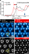
Gate-induced shift of the electronic levels of CVB molecules on a graphene/BN FET device: (a) dI/dV spectra of CVB/graphene/BN at two different gate voltages: VG = 0 V (black trace) and VG = 60 V (red trace). Increasing the gate voltage to VG = 60 V causes a rigid downward shift of the molecular electronic resonances by 0.2 eV, consistent with the gate-induced shift seen in the Dirac point for graphene/BN devices without adsorbed molecules (spectra are normalized by their respective values at VS = 2.6 V). (b) Experimental dI/dV map obtained with VS = 2.4 V and VG = 0 V. (c) Same as (b) except that VG = 60 V. (d) Theoretical local density of states map of the CVB/graphene LUMO state calculated using DFT. (e) Same as (d) except for LUMO+1 state. These maps show that changing the device gate voltage allows the STM to access different molecular orbitals for a fixed sample bias.

References

    1. Schedin F.; Geim A. K.; Morozov S. V.; Hill E. W.; Blake P.; Katsnelson M. I.; Novoselov K. S. Detection of Individual Gas Molecules Adsorbed on Graphene. Nat. Mater. 2007, 6, 652–655. - PubMed
    1. Sojoudi H.; Baltazar J.; Tolbert L. M.; Henderson C. L.; Graham S. Creating Graphene P–N Junctions Using Self-Assembled Monolayers. ACS Appl. Mater. Interfaces 2012, 4, 4781–4786. - PubMed
    1. Peimyoo N.; Li J.; Shang J.; Shen X.; Qiu C.; Xie L.; Huang W.; Yu T. Photocontrolled Molecular Structural Transition and Doping in Graphene. ACS Nano 2012, 6, 8878–8886. - PubMed
    1. Lee B.; Chen Y.; Duerr F.; Mastrogiovanni D.; Garfunkel E.; Andrei E. Y.; Podzorov V. Modification of Electronic Properties of Graphene with Self-Assembled Monolayers. Nano Lett. 2010, 10, 2427–2432. - PubMed
    1. Kim M.; Safron N. S.; Huang C.; Arnold M. S.; Gopalan P. Light-Driven Reversible Modulation of Doping in Graphene. Nano Lett. 2012, 12, 182–187. - PubMed

Publication types