

Review
doi: 10.3390/s140507959.
Recent advances in plasmonic sensors
Affiliations
- PMID: 24803189
- PMCID: PMC4063061
- DOI: 10.3390/s140507959
Item in Clipboard
Review
Recent advances in plasmonic sensors
Sensors (Basel).
.
Abstract
Plasmonic sensing has been an important multidisciplinary research field and has been extensively used in detection of trace molecules in chemistry and biology. The sensing techniques are typically based on surface-enhanced spectroscopies and surface plasmon resonances (SPRs). This review article deals with some recent advances in surface-enhanced Raman scattering (SERS) sensors and SPR sensors using either localized surface plasmon resonances (LSPRs) or propagating surface plasmon polaritons (SPPs). The advances discussed herein present some improvements in SERS and SPR sensing, as well as a new type of nanowire-based SPP sensor.
Figures
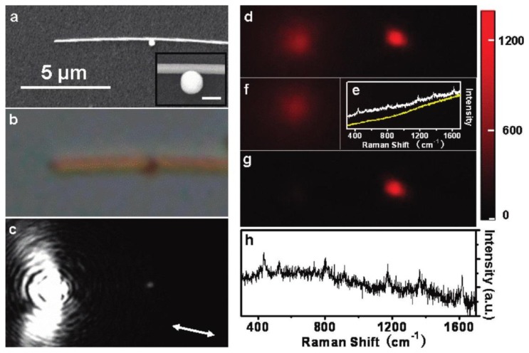
Remote SERS of MGITC excited at the particle/nanowire junction. (a,b) Scanning electron microscope (SEM) and optical images of the structure, respectively; (c) Optical image of SPP propagation excited by 633 nm laser; (d) Raman image at 436 cm−1; (e) Spectra measured at the nanojunction (white) and the excitation spot (yellow); (f) Background fluorescence image of the substrate; (g,h) The corresponding Raman image and SERS spectrum after background correction. Adapted with permission from [49].
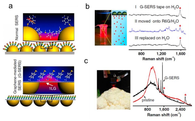
(a) The schemes of normal SERS and G-SERS; (b) Real time and reversible G-SERS characterization of R6G in a 1 × 10⁻⁵ M aqueous solution; (c) Pristine and G-SERS spectra of a cauliflower surface with adsorbed CuPc (soaked in 1 × 10⁻⁵ M CuPc in ethanol for 10 min). “*” marks the enhanced G-band and G'-band features of one-layer graphene. Adapted with permission from [53].
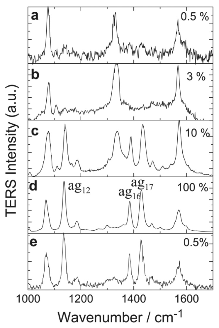
UHV-TERS spectra showing the dimerization of 4-nitrobenzenethiol (4NBT) to dimercaptoazobenzene (DMAB) molecules. Reprinted with permission from [59].
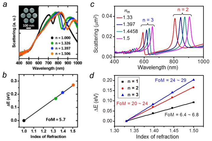
(a,b) Experimental demonstration of LSPR sensing using a gold heptamer. Reproduced with permission from [68]; (c,d) Electromagnetic calculations comparing the sensing performance using different orders (n = 1, 2, 3) of LSPRs on a silver nanorod. Adapted from [71].
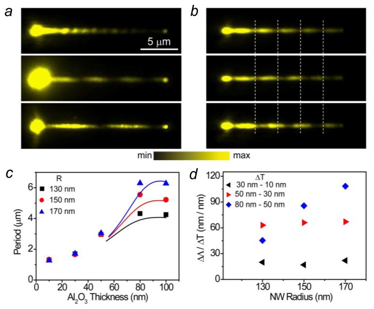
(a) QD emission images for a 155 nm radius NW coated with 15 nm of Al2O3 and QDs measured in air (Top), water (Middle), and oil (Bottom); (b) QD emission images for a 162 nm radius NW with a 50 nm Al2O3 coating measured in air (Top), and then after depositing 5 nm of Al2O3 (Middle), and finally with an additional 5 nm of Al2O3 (Bottom). The white dashed lines are visual guides to show the shift of the plasmon near-field pattern. Scale bar in (a) is for (b) as well; (c) The beat period as a function of Al2O3 coating thickness. The dots are experimental data, and the lines are calculated data; (d) The period change per nanometer of Al2O3 as a function of the nanowire radius (Adapted from [42]).
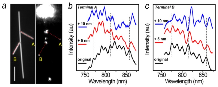
(a) A structure composed of three NWs was illuminated by the supercontinuum light. The length of the scale bar is 5 μm; (b) The emission spectra at the terminal A of the right branch wire for the original structure (black), and for 5 nm (red) and 10 nm (blue) Al2O3 layer deposited, respectively. The dashed lines are visual guides to show the shift of the peaks; (c) The emission spectra at the terminal B of the left branch wire (Adapted from [42]).
References
-
- Zia R., Schuller J.A., Chandran A., Brongersma M.L. Plasmonics: The next chip-scale technology. Mater. Today. 2006;9:20–27.
-
- Ozbay E. Plasmonics: Merging photonics and electronics at nanoscale dimensions. Science. 2006;311:189–193. - PubMed
-
- Atwater H.A., Polman A. Plasmonics for improved photovoltaic devices. Nat. Mater. 2010;9:205–213. - PubMed
-
- Wei H., Xu H.X. Nanowire-based plasmonic waveguides and devices for integrated nanophotonic circuits. Nanophotonics. 2012;1:155–169.
-
- Anker J.N., Hall W.P., Lyandres O., Shah N.C., Zhao J., van Duyne R.P. Biosensing with plasmonic nanosensors. Nat. Mater. 2008;7:442–453. - PubMed
Publication types
MeSH terms
LinkOut - more resources
Full Text Sources
Other Literature Sources
Miscellaneous
