. 2010 Apr 29;114(16):7480-7488.
doi: 10.1021/jp911355q.

Plasmonic Nanoparticles and Nanowires: Design, Fabrication and Application in Sensing

Affiliations

Plasmonic Nanoparticles and Nanowires: Design, Fabrication and Application in Sensing

Tuan Vo-Dinh et al. J Phys Chem C Nanomater Interfaces. .

Abstract

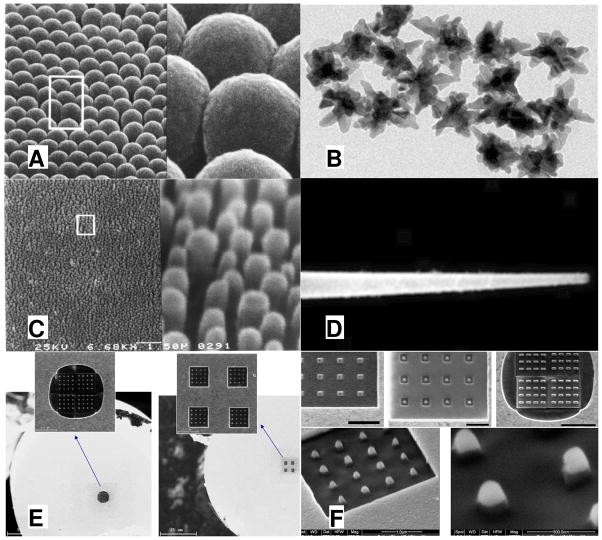
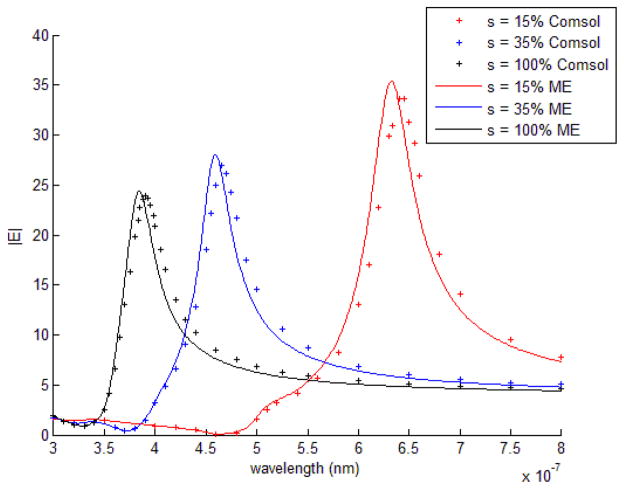
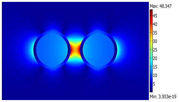
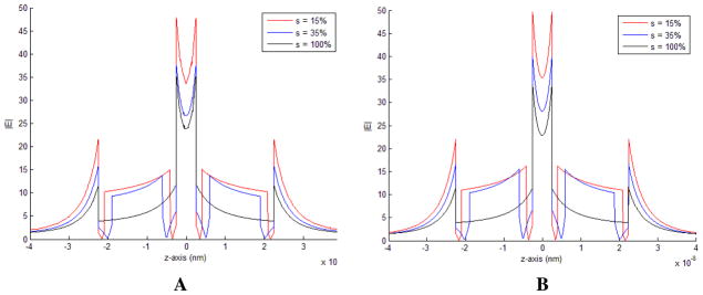
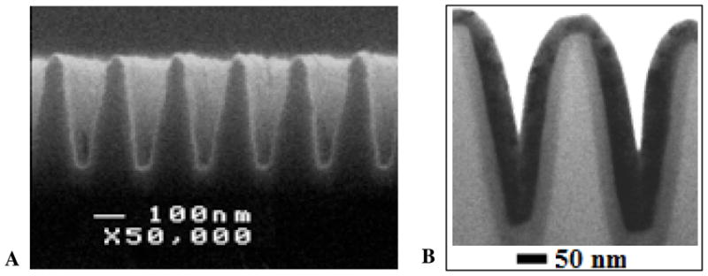
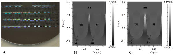
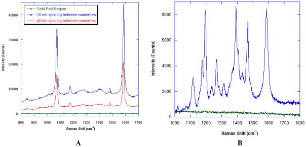
This study involves two aspects of our investigations of plasmonics-active systems: (i) theoretical and simulation studies and (ii) experimental fabrication of plasmonics-active nanostructures. Two types of nanostructures are selected as the model systems for their unique plasmonics properties: (1) nanoparticles and (2) nanowires on substrate. Special focus is devoted to regions where the electromagnetic field is strongly concentrated by the metallic nanostructures or between nanostructures. The theoretical investigations deal with dimers of nanoparticles and nanoshells using a semi-analytical method based on a multipole expansion (ME) and the finite-element method (FEM) in order to determine the electromagnetic enhancement, especially at the interface areas of two adjacent nanoparticles. The experimental study involves the design of plasmonics-active nanowire arrays on substrates that can provide efficient electromagnetic enhancement in regions around and between the nanostructures. Fabrication of these nanowire structures over large chip-scale areas (from a few millimeters to a few centimeters) as well as FDTD simulations to estimate the EM fields between the nanowires are described. The application of these nanowire chips using surface-enhanced Raman scattering (SERS) for detection of chemicals and labeled DNA molecules is described to illustrate the potential of the plasmonics chips for sensing.

Keywords: Plasmonics; SERS; gene diagnostics; metallic nanostructures; molecular sentinel; nanoprobes; surface-enhanced Raman scattering.


Figures

Figure 1
Figure 1
Plasmonics SERS platforms developed for SERS applications: (A) Substrates based on nanosphere arrays coated with silver; (B) Gold nanostars; (C) Nanorod arrays fabricated using submicron lithography and plasma etching; (D) SERS-inducing fiber-optic nanoprobe coated with silver nano-islands; (E) Scanning ion microscope (SIM) image of gold nanopillar arrays developed by FIB milling at the tip of a cleaved gold-coated 4-mode optical fiber (left) and multimode optical fiber (right); (F) (Top) Nanopillars of different geometries. Scale bars are 2 μm, 1 μm, and 2.5 μm respectively. (Bottom) SEM micrograph of a gold nanopillar array taken at 45 degree.
Figure 2
Figure 2
Electric-field magnitude in the particle gap versus wavelength. The solid curves are the calculations using the ME method and the symbols indicate the FEM calculations.
Figure 3
Figure 3
Electric-field magnitude of a 2-D x-z slice through the dimer with 15% shell thickness at a wavelength of 640 nm.
Figure 4
Figure 4
The magnitude of the electric field is shown here along the axis through the three dimer types: (A) FEM calculation using Comsol. (B) ME calculation.
Figure 5
Figure 5
(A) SEM cross-section showing fabrication of a one-dimensional array of triangle-shaped silicon nanowires. The fabrication of silicon nanowires involved deep UV lithography followed by TMAH chemical etching of silicon. (B) TEM cross-section of a gold-coated silicon nanowire SERS substrate: Silicon nanowires (in light grey color) were over-coated with a conformal hafnium oxide layer (in dark grey color) to bridge the gap between the adjacent silicon nanowires in a controlled manner. Finally, a thin layer of gold film (in black color) was evaporated on the hafnium oxide layer to form inverted triangular structures, with sub-10 nm gaps between the metal surfaces.
Figure 6
Figure 6
(A) Picture showing part of a 6 inch wafer-based SERS substrate having gold-coated silicon nanowire structures fabricated across the wafer. (B) FDTD calculations - carried out at 633 nm incident radiation wavelength - showing enhancement of the electric field in the gap between neighboring gold-coated silicon nanowires when the gap at the bottom of neighboring gold-coated silicon nanowires is 5 nm. (C) FDTD calculations as in (B) when the gap at the bottom of neighboring nanowires is 10 nm.
Figure 7
Figure 7
(A) SERS signals from pMBA molecules on gold-coated silicon nanowire substrates, for different spacing between neighboring nanowires in the one-dimensional array of nanowires. The SERS substrate chips were coated with pMBA molecules by dipping the chips in a 1 mM ethanol solution of pMBA. (B) SERS signal from Cy3 dye-labeled breast cancer gene sequence (ERBB2) molecules on gold-coated silicon nanowire substrates.

References

    1. Fleischmann, Hendra PJ, McQuillan AJ. Chem Phys Lett. 1974;26(2):163–166.
    1. Jeanmaire DL, Vanduyne RP. J Electroanal Chem. 1977;84(1):1–20.
    1. Albrecht MG, Creighton JA. J Am Chem Soc. 1977;99(15):5215–5217.
    1. Moskovits M. Rev Modern Phys. 1985;57(3):783–826.
    1. Wokaun A, Gordon JP, Liao PF. Phys Rev Lett. 1982;48(14):957–960.

LinkOut - more resources