

Improved performance and stability in quantum dot solar cells through band alignment engineering
- PMID: 24859641
- PMCID: PMC4110173
- DOI: 10.1038/nmat3984
Improved performance and stability in quantum dot solar cells through band alignment engineering
Abstract
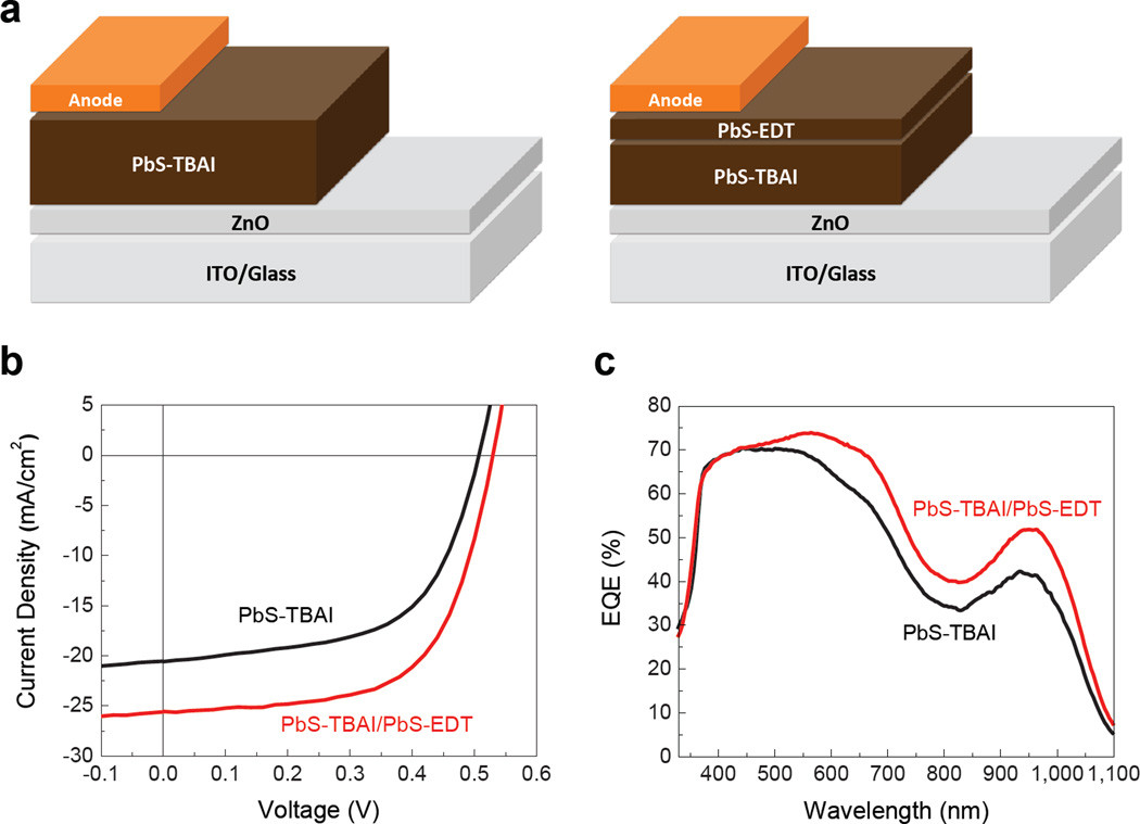
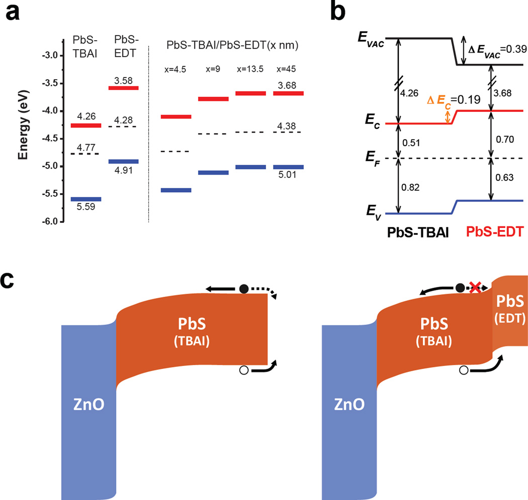
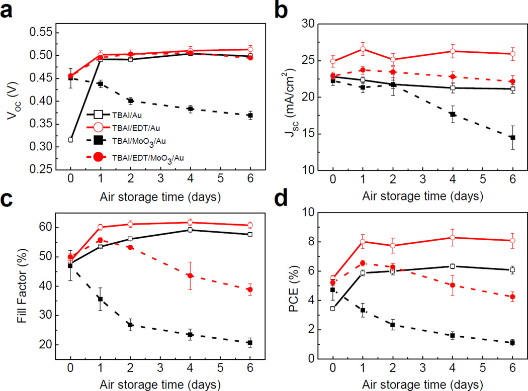
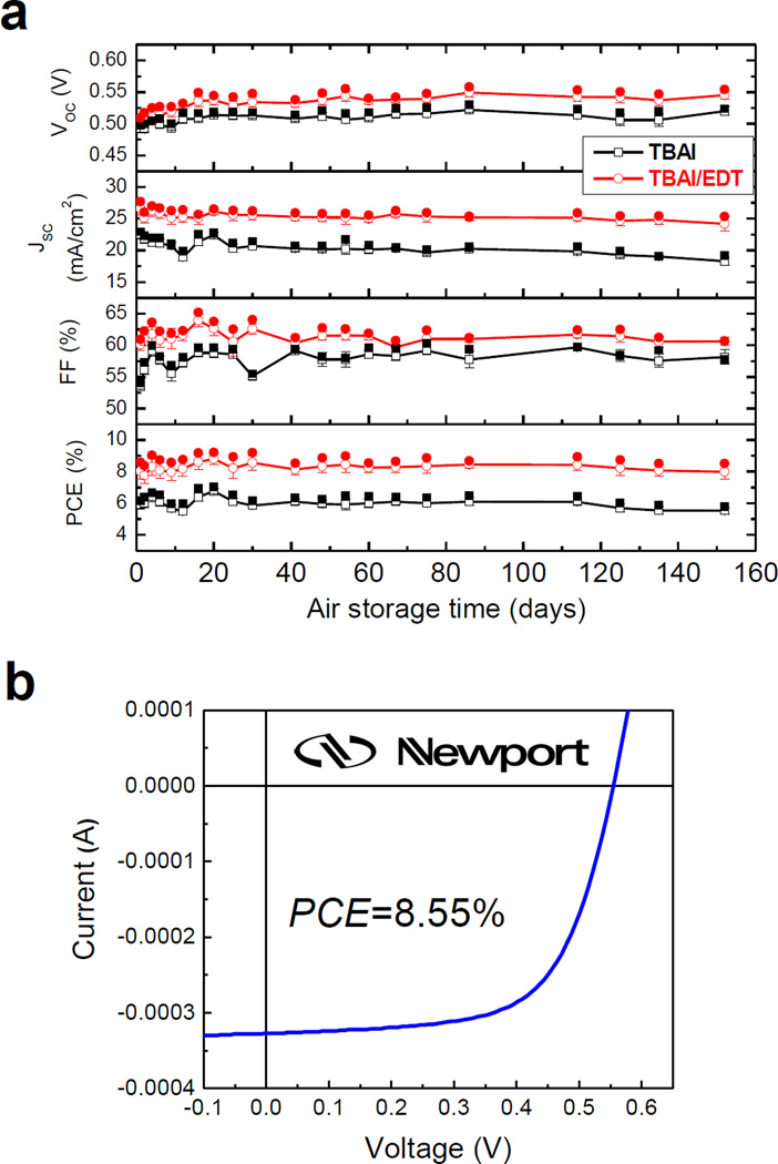
Solution processing is a promising route for the realization of low-cost, large-area, flexible and lightweight photovoltaic devices with short energy payback time and high specific power. However, solar cells based on solution-processed organic, inorganic and hybrid materials reported thus far generally suffer from poor air stability, require an inert-atmosphere processing environment or necessitate high-temperature processing, all of which increase manufacturing complexities and costs. Simultaneously fulfilling the goals of high efficiency, low-temperature fabrication conditions and good atmospheric stability remains a major technical challenge, which may be addressed, as we demonstrate here, with the development of room-temperature solution-processed ZnO/PbS quantum dot solar cells. By engineering the band alignment of the quantum dot layers through the use of different ligand treatments, a certified efficiency of 8.55% has been reached. Furthermore, the performance of unencapsulated devices remains unchanged for over 150 days of storage in air. This material system introduces a new approach towards the goal of high-performance air-stable solar cells compatible with simple solution processes and deposition on flexible substrates.
Figures
References
-
- Graetzel M, Janssen RAJ, Mitzi DB, Sargent EH. Materials interface engineering for solution-processed photovoltaics. Nature. 2012;488:304–312. - PubMed
-
- Wadia C, Alivisatos AP, Kammen DM. Materials availability expands the opportunity for large-scale photovoltaics deployment. Environ. Sci. Technol. 2009;43:2072–2077. - PubMed
-
- Zarghami MH, et al. p-Type PbSe and PbS quantum dot solids prepared with short-chain acids and diacids. ACS Nano. 2010;4:2475–2485. - PubMed
-
- Tang J, et al. Colloidal-quantum-dot photovoltaics using atomic-ligand passivation. Nature Mater. 2011;10:765–771. - PubMed
-
- Ip AH, et al. Hybrid passivated colloidal quantum dot solids. Nature Nanotechnol. 2012;7:577–582. - PubMed
Grants and funding
LinkOut - more resources
Full Text Sources
Other Literature Sources
