. 2014 May 29:5:3991.
doi: 10.1038/ncomms4991.

Imaging atomic-level random walk of a point defect in graphene

Affiliations
Free PMC article

Imaging atomic-level random walk of a point defect in graphene

Jani Kotakoski et al. Nat Commun. .
Free PMC article

Abstract

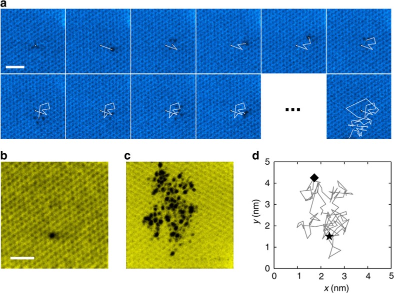
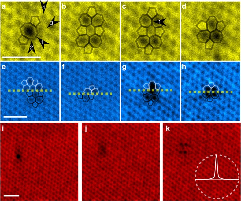
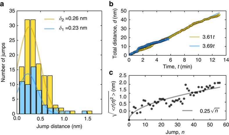
Deviations from the perfect atomic arrangements in crystals play an important role in affecting their properties. Similarly, diffusion of such deviations is behind many microstructural changes in solids. However, observation of point defect diffusion is hindered both by the difficulties related to direct imaging of non-periodic structures and by the timescales involved in the diffusion process. Here, instead of imaging thermal diffusion, we stimulate and follow the migration of a divacancy through graphene lattice using a scanning transmission electron microscope operated at 60 kV. The beam-activated process happens on a timescale that allows us to capture a significant part of the structural transformations and trajectory of the defect. The low voltage combined with ultra-high vacuum conditions ensure that the defect remains stable over long image sequences, which allows us for the first time to directly follow the diffusion of a point defect in a crystalline material.


Figures

Figure 1
Figure 1. Travelling divacancy in graphene.
(a) Ten consecutive frames and the final frame from one image sequence showing the movement of the defect through the lattice. (b) First frame of another image sequence. (c) ‘Superposition’ of all of the frames from the second sequence highlighting the trace of the defect by showing the minimum intensity from the sequence at every pixel. (d) Actual trajectory of the defect in the second sequence, determined by locating the approximate middle point of the defect in every frame. Only those images where the location of the defect was clearly identifiable have been included. The start position is marked with a black star and the last location with a diamond. All scale bars are 1 nm.
Figure 2
Figure 2. Example exposures of the defect.
(ad) Four consecutive frames from the second image sequence. The bonds associated with the defects are highlighted with an overlay. The structure has undergone at least four bond rotations between panels a and b and one between c and d, as marked with the black arrows. (eh) Examples of image scans where the structure changed while scanning exactly at the location of the defect. White and black overlays mark the structure of the defect before and after the change, respectively. (ik) Three consecutive frames from the second image sequence. The defect appears in the V2(585) configuration in panel i, but disappears for the duration of the next scan resulting in panel j, before appearing again in panel k, in the V2(5555-6-7777) configuration. The darker area within panel j presumably corresponds to the area where the defect is located, although it avoids detection (locations of all atoms belonging to the pristine lattice can be identified). In panel k, a circle with radius of 1.5 nm is drawn for scale with the experimentally obtained probe shape. In these panels the complete field of view is shown. The scale bars are 1 nm.
Figure 3
Figure 3. Determination of the probe shape.
(a) Unprocessed (but coloured) image of a graphene edge. (b) Line profile obtained from the area shaded in panel a in the direction of the arrow along with a simulated line profile calculated assuming that the graphene edge is a step function and convoluting it with a probe that consists of three 2D Gaussians. The graphene edge position was set to the zero of the x axis. The s.d. for the Gaussians (σ1, σ2 and σ3) were obtained via manual fitting, with an estimated accuracy of ca. 10%. (c) One-dimensional profile of the probe consisting of the three Gaussians. Vacuum intensity was set to zero.
Figure 4
Figure 4. Statistical analysis of a random walk.
(a) Histograms of all of the jump distances by the defect in the two image sequences. The lines show normal distributions fitted to the data. (b) Corresponding cumulative total distance travelled by the defect as a function of time. The lines are fits to the data. (c) Root-mean-square distance of the defect from the starting position as a function of time. The solid line is a fit to the data.

References

    1. Hashimoto A., Suenaga K., Gloter A., Urita K. & Iijima S. Direct evidence for atomic defects in graphene layers. Nature 430, 870–873 (2004). - PubMed
    1. Meyer J. C. et al. Direct imaging of lattice atoms and topological defects in graphene membranes. Nano Lett. 8, 3582–3586 (2008). - PubMed
    1. Jin C., Lin F., Suenaga K. & Iijima S. Fabrication of a freestanding boron nitride single layer and its defect assignments. Phys. Rev. Lett. 102, 195505 (2009). - PubMed
    1. Meyer J. C., Chuvilin A., Algara-Siller G., Biskupek J. & Kaiser U. Selective sputtering and atomic resolution imaging of atomically thin boron nitride membranes. Nano Lett. 9, 2683–2689 (2009). - PubMed
    1. Komsa H.-P. et al. Two-dimensional transition metal dichalcogenides under electron irradiation: defect production and doping. Phys. Rev. Lett. 109, 035503 (2012). - PubMed

Publication types