

Temporal and spatial temperature measurement in insulator-based dielectrophoretic devices
- PMID: 24889741
- PMCID: PMC4082381
- DOI: 10.1021/ac501083h
Temporal and spatial temperature measurement in insulator-based dielectrophoretic devices
Abstract
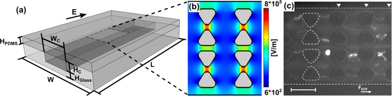
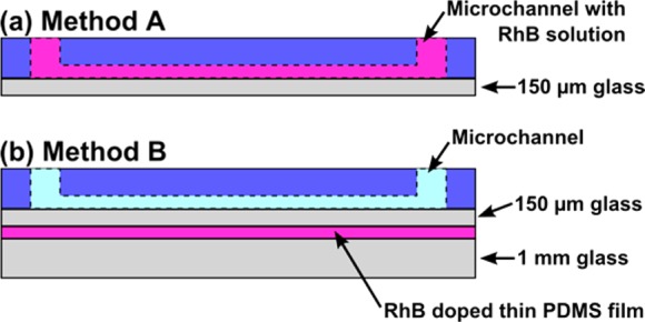
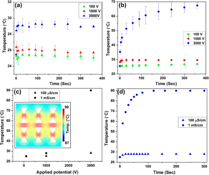
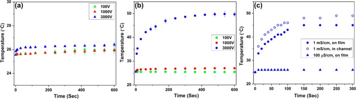
Insulator-based dielectrophoresis is a relatively new analytical technique with a large potential for a number of applications, such as sorting, separation, purification, fractionation, and preconcentration. The application of insulator-based dielectrophoresis (iDEP) for biological samples, however, requires the precise control of the microenvironment with temporal and spatial resolution. Temperature variations during an iDEP experiment are a critical aspect in iDEP since Joule heating could lead to various detrimental effects hampering reproducibility. Additionally, Joule heating can potentially induce thermal flow and more importantly can degrade biomolecules and other biological species. Here, we investigate temperature variations in iDEP devices experimentally employing the thermosensitive dye Rhodamin B (RhB) and compare the measured results with numerical simulations. We performed the temperature measurement experiments at a relevant buffer conductivity range commonly used for iDEP applications under applied electric potentials. To this aim, we employed an in-channel measurement method and an alternative method employing a thin film located slightly below the iDEP channel. We found that the temperature does not deviate significantly from room temperature at 100 μS/cm up to 3000 V applied such as in protein iDEP experiments. At a conductivity of 300 μS/cm, such as previously used for mitochondria iDEP experiments at 3000 V, the temperature never exceeds 34 °C. This observation suggests that temperature effects for iDEP of proteins and mitochondria under these conditions are marginal. However, at larger conductivities (1 mS/cm) and only at 3000 V applied, temperature increases were significant, reaching a regime in which degradation is likely to occur. Moreover, the thin layer method resulted in lower temperature enhancement which was also confirmed with numerical simulations. We thus conclude that the thin film method is preferable providing closer agreement with numerical simulations and further since it does not depend on the iDEP channel material. Overall, our study provides a thorough comparison of two experimental techniques for direct temperature measurement, which can be adapted to a variety of iDEP applications in the future. The good agreement between simulation and experiment will also allow one to assess temperature variations for iDEP devices prior to experiments.
Figures

Similar articles
-
Joule heating effects in optimized insulator-based dielectrophoretic devices: An interplay between post geometry and temperature rise.Electrophoresis. 2019 May;40(10):1408-1416. doi: 10.1002/elps.201800490. Epub 2019 Mar 27. Electrophoresis. 2019. PMID: 30883810
-
Joule heating-enabled electrothermal enrichment of nanoparticles in insulator-based dielectrophoretic microdevices.Electrophoresis. 2021 Mar;42(5):626-634. doi: 10.1002/elps.202000192. Epub 2020 Sep 28. Electrophoresis. 2021. PMID: 32935875
-
On the recent developments of insulator-based dielectrophoresis: A review.Electrophoresis. 2019 Feb;40(3):358-375. doi: 10.1002/elps.201800285. Epub 2018 Aug 30. Electrophoresis. 2019. PMID: 30112789 Review.
-
Characterization of electrokinetic mobility of microparticles in order to improve dielectrophoretic concentration.Anal Bioanal Chem. 2009 May;394(1):293-302. doi: 10.1007/s00216-009-2626-y. Epub 2009 Feb 4. Anal Bioanal Chem. 2009. PMID: 19190896
-
Insulator Based Dielectrophoresis: Micro, Nano, and Molecular Scale Biological Applications.Sensors (Basel). 2020 Sep 7;20(18):5095. doi: 10.3390/s20185095. Sensors (Basel). 2020. PMID: 32906803 Free PMC article. Review.
Cited by
-
Localized Dielectric Loss Heating in Dielectrophoresis Devices.Sci Rep. 2019 Dec 12;9(1):18977. doi: 10.1038/s41598-019-55031-y. Sci Rep. 2019. PMID: 31831755 Free PMC article.
-
Protein dielectrophoresis and the link to dielectric properties.Bioanalysis. 2015;7(3):353-71. doi: 10.4155/bio.14.306. Bioanalysis. 2015. PMID: 25697193 Free PMC article. Review.
-
Particle trapping in electrically driven insulator-based microfluidics: Dielectrophoresis and induced-charge electrokinetics.Electrophoresis. 2021 Dec;42(23):2445-2464. doi: 10.1002/elps.202100123. Epub 2021 Jun 15. Electrophoresis. 2021. PMID: 34081787 Free PMC article. Review.
-
High throughput protein nanocrystal fractionation in a microfluidic sorter.Anal Chem. 2015 Apr 21;87(8):4159-67. doi: 10.1021/acs.analchem.5b00589. Epub 2015 Apr 7. Anal Chem. 2015. PMID: 25794348 Free PMC article.
-
Deterministic Ratchet for Sub-micrometer (Bio)particle Separation.Anal Chem. 2018 Apr 3;90(7):4370-4379. doi: 10.1021/acs.analchem.7b03774. Epub 2018 Mar 23. Anal Chem. 2018. PMID: 29506379 Free PMC article.
References
Publication types
MeSH terms
Grants and funding
LinkOut - more resources
Full Text Sources
Other Literature Sources
Molecular Biology Databases
