. 2014 May 3;9(1):207.
doi: 10.1186/1556-276X-9-207. eCollection 2014.

Gold nanoparticles grown inside carbon nanotubes: synthesis and electrical transport measurements

Affiliations

Gold nanoparticles grown inside carbon nanotubes: synthesis and electrical transport measurements

Rodrigo A Segura et al. Nanoscale Res Lett. .

Abstract

The hybrid structures composed of gold nanoparticles and carbon nanotubes were prepared using porous alumina membranes as templates. Carbon nanotubes were synthesized inside the pores of these templates by the non-catalytic decomposition of acetylene. The inner cavity of the supported tubes was used as nanoreactors to grow gold particles by impregnation with a gold salt, followed by a calcination-reduction process. The samples were characterized by transmission electron microscopy and X-ray energy dispersion spectroscopy techniques. The resulting hybrid products are mainly encapsulated gold nanoparticles with different shapes and dimensions depending on the concentration of the gold precursor and the impregnation procedure. In order to understand the electronic transport mechanisms in these nanostructures, their conductance was measured as a function of temperature. The samples exhibit a 'non-metallic' temperature dependence where the dominant electron transport mechanism is 1D hopping. Depending on the impregnation procedure, the inclusion of gold nanoparticles inside the CNTs can introduce significant changes in the structure of the tubes and the mechanisms for electronic transport. The electrical resistance of these hybrid structures was monitored under different gas atmospheres at ambient pressure. Using this hybrid nanostructures, small amounts of acetylene and hydrogen were detected with an increased sensibility compared with pristine carbon nanotubes. Although the sensitivity of these hybrid nanostructures is rather low compared to alternative sensing elements, their response is remarkably fast under changing gas atmospheres.

Keywords: 81.07.-b; 81.07.De; 81.15.Gh; Au-CNT hybrid; Carbon nanotubes; Electric transport; Gas sensing.


Figures
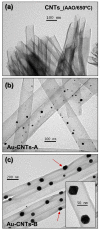
Figure 1
Figure 1
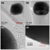
TEM images of pure CNTs and Au-CNT hybrids. (a) Pure CNTs prepared using the AAO template. (b) Au-CNT hybrids prepared by dip-coating method. (c) Au-CNT hybrids prepared by drop-casting. Important deformations are indicated by red arrows.
Figure 2
Figure 2
HRTEM images of the hybrid nanostructures prepared by dip-coating (Au-CNT-A). (a-d) Individual gold nanoparticles. (a) An onion-like carbon shell surrounding the AuNP. (b, c) The interplanar spacing, consistent with Au fcc, is highlight with red lines. The insert in (c) shows the shape of a decahedral object to allow comparison with the HRTEM image.
Figure 3
Figure 3
HRTEM images of the hybrid nanostructures prepared by drop-casting (Au-CNT-B). (a-c) The surrounding C shell and the AuNP-CNT interface can be observed. (d) Interlayer spacing of 0.235 nm is consistent with fcc (111) planes in Au.
Figure 4
Figure 4
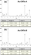
EDS analysis of the hybrid nanostructures prepared by (a) dip-coating and (b) drop-casting.
Figure 5
Figure 5
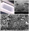
Images of the IME chip and Au-CNT samples deposited over IME chip. (a) Optical image of the IME chip. (b, c) Representative SEM images of Au-CNT samples deposited over IME chip.
Figure 6
Figure 6
Plots of ln(G) for the samples CNTs_(AAO/650°C), Au-CNTs-A, and Au-CNTs-B as a function of T−1/2. In addition to the measured data (open symbols), illustrative error bars have been included for each sample.
Figure 7
Figure 7
HRTEM images, SAED patterns, and average Raman spectra from purified and annealed CNTs. (a, b) Representative HRTEM micrographs of tube walls of the samples CNTs_(AAO/650°C) and CNTs-2900 K, respectively. The inserts in (a) and (b) are the diffraction patterns taken in the respective micrograph. (c) The average Raman spectra obtained from several measurements on different locations on the samples.
Figure 8
Figure 8
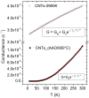
Temperature dependence of the conductance for purified and annealed CNTs. Temperature dependence of the conductance (G) measured at zero bias voltage for the samples CNTs-2900 K (green open circles) and CNTs_(AAO/650°C) (black squares). The red lines are the fit to the corresponding models; see text for further details.
Figure 9
Figure 9
Changes in resistance of CNT_(AAO/650°C) sample deposited on IME chip due to different environmental conditions. In zone (1), vacuum/air cycles were performed (vacuum level is close 68 kΩ). In zone (2), air was replaced by argon. In zone (3), the chamber was pumped, and in zone (4), vacuum/Ar cycles were performed.
Figure 10
Figure 10
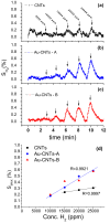
Sensing response of CNT and Au-CNT samples towards the detection of acetylene (C2H2). Response of pure CNTs (a) and response of hybrid Au-CNT samples prepared by dip-coating (b) and drop-casting (c). Plot of the maximum sensitivity value for each peak as a function of C2H2 concentration (d). The solid lines in d graph are linear fits to the corresponding data points.
Figure 11
Figure 11
Sensing responses of CNT and Au-CNT samples towards the detection of hydrogen (H2). Behaviour of pure CNTs (a) and hybrid Au-CNT samples prepared by dip-coating (b) and drop-casting (c). Maximum sensitivity value for each peak as a function of H2 concentration (d). Solid line in d graph represents the linear fit to these data points.

References

    1. Baumberg JJ. Breaking the mould: casting on the nanometer scale. Nat Mater. 2006;9:2–5. doi: 10.1038/nmat1562. - DOI
    1. Vlasov YA, Bo XZ, Sturm JC, Norris DJ. On-chip natural assembly of silicon photonic bandgap crystals. Nature. 2001;9:289–293. doi: 10.1038/35104529. - DOI - PubMed
    1. Hu Z, Tian M, Nysten B, Jonas AM. Regular arrays of highly ordered ferroelectric polymer nanostructures for non-volatile low-voltage memories. Nat Mat. 2009;9:62–67. doi: 10.1038/nmat2339. - DOI - PubMed
    1. Bita I, Yang JKW, Jung YS, Ross CA, Thomas EL, Berggren KK. Graphoepitaxy of self-assembled block copolymers on two-dimensional periodic patterned templates. Science. 2008;9:939–943. doi: 10.1126/science.1159352. - DOI - PubMed
    1. Ruiz R, Kang H, Detcheverry FA, Dobisz E, Kercher DS, Albrecht TR, De Pablo JJ, Nealey PF. Density multiplication and improved lithography by directed block copolymer assembly. Science. 2008;9:936–939. doi: 10.1126/science.1157626. - DOI - PubMed